

Heat has always been the enemy of electronics. In High Current applications, this enemy grows stronger. Components that dissipate significant power generate thermal gradients across circuit boards, and if that heat isn't managed effectively, reliability suffers. The solution for many designers involves Thermal Vias—copper-plated holes that conduct heat away from components through the board structure. But thermal via design isn't simple. Array spacing, via geometry, and fill strategies all influence how effectively heat transfers. Getting these parameters right separates designs that survive field use from those that fail prematurely.
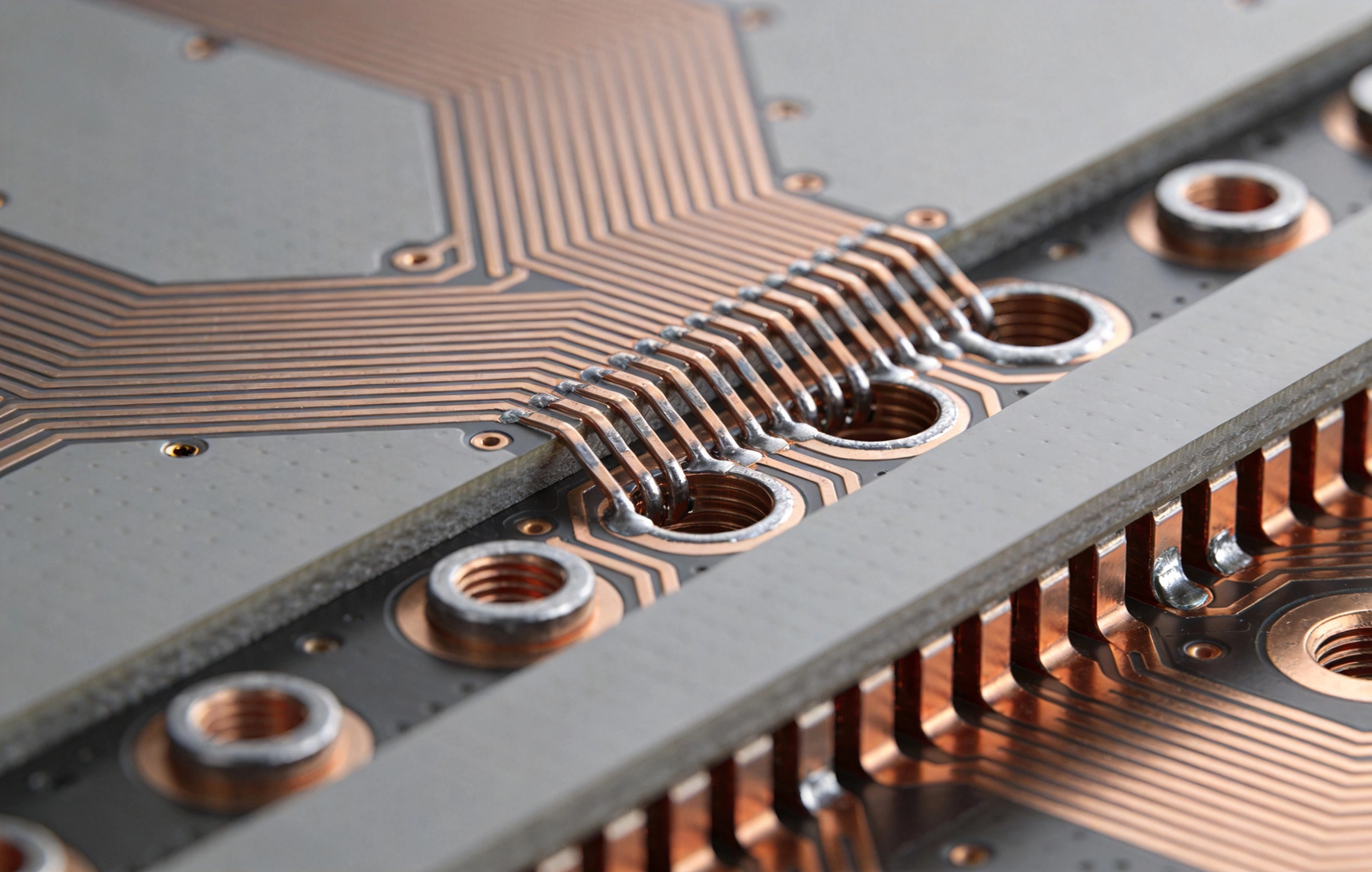
This article explores the principles behind thermal via design, practical spacing guidelines, and the tradeoffs engineers face when optimizing heat transfer efficiency. Whether you're designing motor controllers, power converters, or Led Drivers, understanding thermal via optimization helps create more reliable products.
Thermal Vias serve as heat conduits through the PCB stackup. When a component generates heat at its package, that thermal energy flows through the copper pads, into the via barrels, and distributes across internal planes or to the board surface exposed to ambient air. The mechanism sounds straightforward, but achieving effective thermal transfer requires attention to multiple parameters.
In High Current applications, Thermal Management becomes even more critical. Components like MOSFETs, voltage regulators, and power amplifiers often operate at current levels that generate substantial heat. Without adequate thermal paths, junction temperatures rise, reducing component lifetime or causing immediate failure. Designers must balance thermal performance against board space, Manufacturing Cost, and routing constraints.
Thermal via arrays typically connect component thermal pads to large copper areas on adjacent layers, ground planes, or dedicated heatsink attachments. The effectiveness of this thermal path depends on the number of vias, their geometry, spacing, and the thermal conductivity of the PCB materials.
Thermal resistance describes how much temperature rise occurs per unit of power dissipated. Lower thermal resistance means better heat transfer. For via arrays, thermal resistance depends on via geometry, copper plating thickness, and the thermal conductivity of the dielectric material surrounding the vias.
The basic thermal resistance of a single via can be approximated using cylindrical heat conduction models. However, via arrays behave differently because heat flows from multiple vias into shared planes. The thermal interaction between adjacent vias affects overall array performance. When vias are spaced closely, their thermal fields overlap, reducing the effective heat transfer per via.
Understanding this interaction helps designers optimize spacing. Too wide spacing wastes potential thermal transfer area. Too narrow spacing creates overlapping thermal fields with diminishing returns. The optimal spacing balances thermal performance against manufacturing constraints and board routing requirements.
Total thermal resistance from a component junction to ambient includes multiple contributions. The interface resistance between component and PCB matters first. Then comes spreading resistance through copper planes, conduction resistance through vias, and finally convection from exposed surfaces.
Via barrel resistance dominates in standard thermal via configurations. Copper thermal conductivity is roughly 400 W/mK, much higher than FR-4 substrate at 0.3 W/mK. This conductivity difference means heat prefers copper paths. Maximizing copper cross-section in the thermal path reduces resistance.
Plating thickness directly impacts thermal via performance. Standard PCB plating of 25 microns provides limited thermal conduction. Thick plating options—1 oz, 2 oz, or heavier—substantially improve thermal performance. For high current applications requiring excellent Thermal Management, Heavy Copper plating often justifies the additional cost.
General guidelines suggest thermal via spacing between 1-3 times the via pitch diameter. However, optimal spacing depends on specific requirements. Lower spacing densities provide better heat transfer but consume more board area. Higher densities may offer diminishing returns.
A common starting point uses 1mm pitch spacing for standard thermal applications. This provides good thermal spreading without excessive via count. For high power applications, tighter spacing of 0.8mm or even 0.5mm may be appropriate. Wider spacing of 1.5-2mm can work for lower-power components with acceptable temperature rises.
The trade-off involves thermal resistance versus board area. Each via consumes some copper budget on each layer. Dense arrays require more routing channel on surrounding layers, potentially complicating layout. Designers must balance thermal performance against routing flexibility and Manufacturing Cost.
When thermal vias are placed closely together, their individual thermal fields interact. Each via creates a temperature gradient radiating outward from its barrel. Adjacent vias' thermal gradients overlap, creating a combined thermal zone with modified temperature distribution.
At very tight spacing, thermal overlap reduces the effectiveness of individual vias. Adding more vias beyond a certain density provides minimal additional thermal improvement because the vias are essentially competing for the same thermal pathways. Understanding this helps avoid over-designing thermal arrays.
Analysis tools or thermal simulation help identify optimal spacing for specific applications. FEM Thermal Analysis can model via arrays accurately, accounting for material properties and boundary conditions. For many practical designs, empirically-derived spacing guidelines provide adequate results without requiring detailed simulation.
Via diameter affects both thermal performance and manufacturing considerations. Larger diameter vias provide lower thermal resistance because they have greater copper cross-section. However, larger vias consume more board area and may create routing challenges.
Standard via sizes from 0.3mm to 0.8mm diameter serve most thermal via applications. Smaller vias like 0.2mm or 0.15mm can be used in high-density designs but may have limited plating thickness that reduces thermal performance. Larger vias exceeding 1.0mm may be overkill unless extreme thermal transfer is required.
Thermal vias in pad versus thermal vias outside pad represents another consideration. Placing vias directly in component thermal pads provides direct thermal connection but requires careful pad design to prevent Solder Wicking. Thermal vias placed outside the pad but connected through thermal planes add spreading resistance but avoid solder concerns.
Via length depends on PCB stackup. Longer thermal paths through thick boards create higher thermal resistance. For high current applications, minimizing thermal path length improves heat transfer.
Blind and buried vias can reduce thermal path length by connecting only relevant layers. A blind thermal via from the component layer directly to the ground plane bypasses intermediate layers. This approach improves thermal performance but adds manufacturing complexity and cost.
Microvias offer advantages for thermal management in HDI designs. Their small diameter and laser-formed profiles create efficient thermal paths with minimal layer engagement. However, microvia technology adds cost and may have plating limitations compared to through-hole vias.
Standard thermal vias feature copper plating on barrel walls with no fill material. This approach provides thermal conduction through the copper barrel while maintaining the drilled hole for plating processing. Manufacturing is straightforward and cost-effective.
Thermal resistance of standard plated vias depends primarily on copper cross-section and plating thickness. For applications requiring moderate thermal improvement, standard vias often suffice. The manufacturing simplicity and cost advantage make them attractive for cost-sensitive products.
However, standard vias have air gaps in their centers. Air thermal conductivity of roughly 0.025 W/mK is much lower than copper, so the hollow center provides minimal thermal contribution. The effective thermal conductivity of a standard via is essentially the copper fraction multiplied by copper's thermal conductivity.
Copper-filled vias eliminate the air gap by plating copper completely through the barrel. This approach dramatically improves thermal performance—filled vias achieve thermal conductivity approaching solid copper. The thermal resistance improvement typically ranges from 3x to 10x compared to standard plated vias.
Manufacturing copper-filled vias requires additional processing: either multiple plating passes, conductive fill followed by overplate, or specialized fill processes. The additional cost is significant but justified for high-power applications where thermal performance is critical.
Thermal vias can also be filled with thermal epoxy compounds. Thermally conductive epoxies typically achieve 1-5 W/mK conductivity, better than air but not as good as copper. Epoxy fill costs less than copper fill while still providing meaningful thermal improvement over hollow vias.
Metal-core PCB technology offers another thermal management approach. Metal-core boards substitute aluminum or copper substrates for standard FR-4, providing thermal conductivity of 1-200 W/mK depending on core material. Thermal vias through metal-core substrates can achieve exceptional heat spreading.
Metal-core designs suit high-power applications like LED lighting, motor drives, and power supplies where thermal management is the primary constraint. The cost premium and design limitations of metal-core boards restrict their use to applications where thermal performance outweighs other considerations.
The component Thermal Pad size determines how many thermal vias can be placed and how effectively they connect to the component. Larger thermal pads accommodate more vias but may conflict with routing requirements or exceed recommended footprint dimensions.
A common guideline places thermal vias within the component Thermal Pad footprint, with spacing designed to maintain adequate solder mask dams between vias. Via-in-pad designs require solder mask covering or specific fill processes to prevent solder from wicking down the via barrel during reflow.
Thermal pad connection to internal planes should use multiple thermal vias with adequate spacing to minimize spreading resistance. The thermal path from pad to plane should be as direct as possible, avoiding narrow thermal bottlenecks that limit heat transfer.
Connecting thermal vias to ground planes leverages the large copper areas available on power and ground planes. These planes distribute heat across the board surface, where convection and radiation transfer it to ambient air. The effectiveness of this thermal spreading depends on plane Copper Weight and exposed surface area.
Thermal Relief Patterns connecting thermal vias to planes create thermal resistance at the connection point. For thermal vias, solid connections without thermal reliefs provide better thermal performance. However, manufacturing constraints may require some relief geometry to ensure reliable plating.
Dedicated thermal planes—copper areas not used for electrical routing—can be added specifically for thermal management. These islands of copper provide spreading area without affecting Electrical Design. This approach trades routing flexibility for thermal performance.
For extreme thermal loads, thermal vias can connect to external heatsinks through mounting holes or dedicated thermal pads. Adding heatsink attachment expands the thermal dissipation path beyond what the PCB alone can manage. This approach is common in motor drives, audio amplifiers, and other high-power applications.
Thermal interface materials (TIM) between the PCB thermal pad and heatsink fill microscopic air gaps, improving thermal transfer at the interface. TIM selection affects overall thermal resistance. Higher conductivity materials provide better performance but may cost more or have application constraints.
Mechanical mounting considerations affect thermal performance. Uneven mounting pressure, gaps in the interface, or poor surface contact all degrade thermal transfer. Designing for reliable thermal interface requires attention to flatness tolerances, mounting hardware, and interface material selection.
Thermal simulation using Finite Element Analysis (FEA) tools can model thermal via array performance accurately. These tools account for material properties, boundary conditions, and geometric complexity that analytical methods cannot capture. For critical designs, simulation investment is often justified.
Simulation setup requires accurate material properties, appropriate mesh density, and realistic boundary conditions. The thermal conductivity of PCB materials varies with temperature and composition—using generic values may introduce errors. Calibration against test measurements improves confidence in simulation results.
Physical testing remains important despite simulation capabilities. Thermocouple measurements, thermal imaging, and functional testing validate that designs achieve intended thermal performance. prototypes enable design refinement before committing to production tooling. Many reliability failures trace to thermal issues not captured in simulation—testing catches what modeling misses.
Thermal via effectiveness depends on plating quality. Voids in plating, thin copper coverage, or barrel cracks create thermal resistance that defeats design intent. Working with manufacturers who understand high-reliability plating requirements helps ensure consistent thermal via performance.
IPC standards define acceptance criteria for via quality. Class 3 requirements for high-reliability applications specify minimum plating thickness and continuity testing. For thermal vias where performance depends on copper cross-section, these requirements matter even more than for standard signal vias.
Acceptance testing of thermal vias can include cross-section analysis, pull testing, and thermal resistance measurement. These tests add cost but provide confidence that manufacturing process variation hasn't compromised thermal performance. Critical applications may require 100% thermal via testing rather than sampling inspection.
Thermal via costs scale with complexity. Standard plated vias cost only slightly more than signal vias of similar size. Copper-filled vias add significant processing cost per via. Metal-core boards have substantial material and manufacturing premiums. Designers should understand cost implications when selecting thermal strategies.
High via counts increase drilling and plating time, raising manufacturing costs. Optimizing via array size and spacing avoids unnecessary cost while achieving thermal targets. Sometimes designing for slightly higher thermal resistance allows fewer vias, reducing cost more than the thermal penalty.
Dense via arrays may require special processing like back-drilling to remove stubs that cause signal integrity issues in high-speed applications. While thermal vias often don't require back-drilling, designs with mixed thermal and high-speed requirements may need both thermal optimization and signal integrity consideration.
Placing thermal vias under components without connecting them to thermal planes wastes vias. Each thermal via should have a defined path to heat spreading surfaces. Orphaned thermal vias may look helpful but provide minimal actual thermal benefit.
Insufficient via count fails to achieve intended thermal performance. Conservative designs may include thermal arrays adequate for prototype testing but inadequate for production variation or worst-case thermal conditions. Designing for margin helps ensure reliable performance across manufacturing and environmental variation.
Ignoring thermal interface resistance between the component and PCB limits thermal optimization. The interface between component case and board surface may be the dominant thermal resistance in some packages. Thermal interface materials, mounting pressure, and surface preparation all affect this resistance.
Assuming ambient temperature instead of actual worst-case conditions leads to under-designed thermal management. Production equipment may operate in elevated ambient temperatures. Design margins should account for the actual environment, not ideal laboratory conditions.
Optimal spacing depends on thermal load, board properties, and performance requirements. A practical starting point is 1mm pitch for moderate thermal loads, 0.5-0.8mm for higher power density, and tighter spacing only for extreme applications where simulation or testing validates the benefit. Always balance thermal performance against board area and manufacturing constraints.
Copper-filled thermal vias provide 3-10x better thermal performance than standard plated vias but add significant cost. Use filled vias when thermal performance is critical and the cost premium is acceptable. Standard plated vias work for moderate thermal loads where cost sensitivity is higher. Thermal epoxy fill offers middle-ground performance at moderate cost.
Requirements vary with MOSFET power dissipation, package type, and acceptable temperature rise. A typical guideline ranges from 9 to 25 thermal vias for D2PAK or TO-263 packages. High-power applications may need more. Thermal simulation or measurement validates adequacy for specific designs.
Thermal vias carrying only DC currents don't affect high-speed signal integrity. However, thermal via placement near high-speed signal traces can create impedance discontinuities or couple noise. Keep thermal vias away from critical signal routing, or use careful via-in-pad techniques for dense high-speed designs.
Standard 25-micron (1 oz) plating works for many thermal via applications. High current thermal vias benefit from heavier plating—2 oz (50 microns) or more significantly reduces thermal resistance. For extreme thermal requirements, work with manufacturers to specify plating thickness that meets thermal and manufacturing requirements.
Thermal via design for high current PCBs requires balancing multiple factors: thermal performance, board space, manufacturing cost, and reliability requirements. Understanding thermal resistance fundamentals, via geometry effects, and spacing optimization helps engineers create effective thermal management solutions.
No single approach works for every application. Low-cost products may accept moderate thermal performance from standard plated vias. High-reliability systems may justify copper-filled via costs to achieve thermal targets. The right solution depends on specific requirements, not universal rules.
Design iteration with thermal simulation, prototype testing, and manufacturing collaboration refines thermal via strategies into robust implementations. Investing in proper thermal management pays dividends in product reliability, performance, and customer satisfaction. The challenge of heat transfer remains fundamental to electronics—thermal via optimization is one tool in the comprehensive thermal management toolkit.
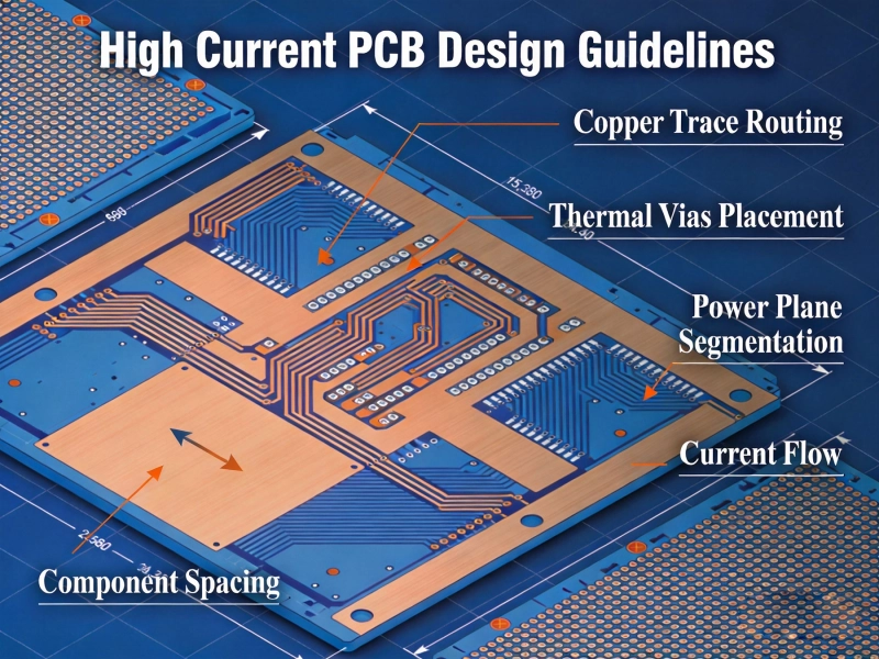
High Current PCB Design GuidelinesMay/21/2026

High Current PCB Design for Medical Imaging EquipmentSeptember/10/2026
High Current PCB Design for Uninterruptible Power Supplies (UPS)September/02/2026
High Current PCB Design for Aerospace Power DistributionSeptember/08/2026
High Current PCB Trace Width Calculator: The Ultimate Engineering GuideMay/20/2026

High Current PCB Design for High-Frequency Switching RegulatorsSeptember/04/2026

High Current PCB Design for Drone ESCs: Minimizing Loop InductanceAugust/03/2026
High Current PCB Design for High-Power LED DriversAugust/12/2026