

Castellated holes, also called edge-plated half-holes or stamp holes, have become a popular connection method for High-current Pcb modules including power supplies, battery management systems, and motor drivers. Unlike through-hole connectors or soldered wires, castellated holes allow modules to be surface mounted directly onto a carrier board, creating a compact, low-profile connection that saves space and simplifies assembly. However, when these holes are used to carry high currents, their Current Carrying Capacity and long-term solder reliability become critical design considerations that are often underestimated.
Many design teams assume castellated holes have similar current ratings to standard through-hole vias of the same size, but this is rarely the case. The unique geometry of castellated holes creates structural and thermal characteristics that affect both their maximum current capacity and their long-term reliability under load. Understanding these differences, and following proven design and manufacturing guidelines, ensures your castellated hole connections perform reliably for the full service life of your product without overheating or solder joint failure.
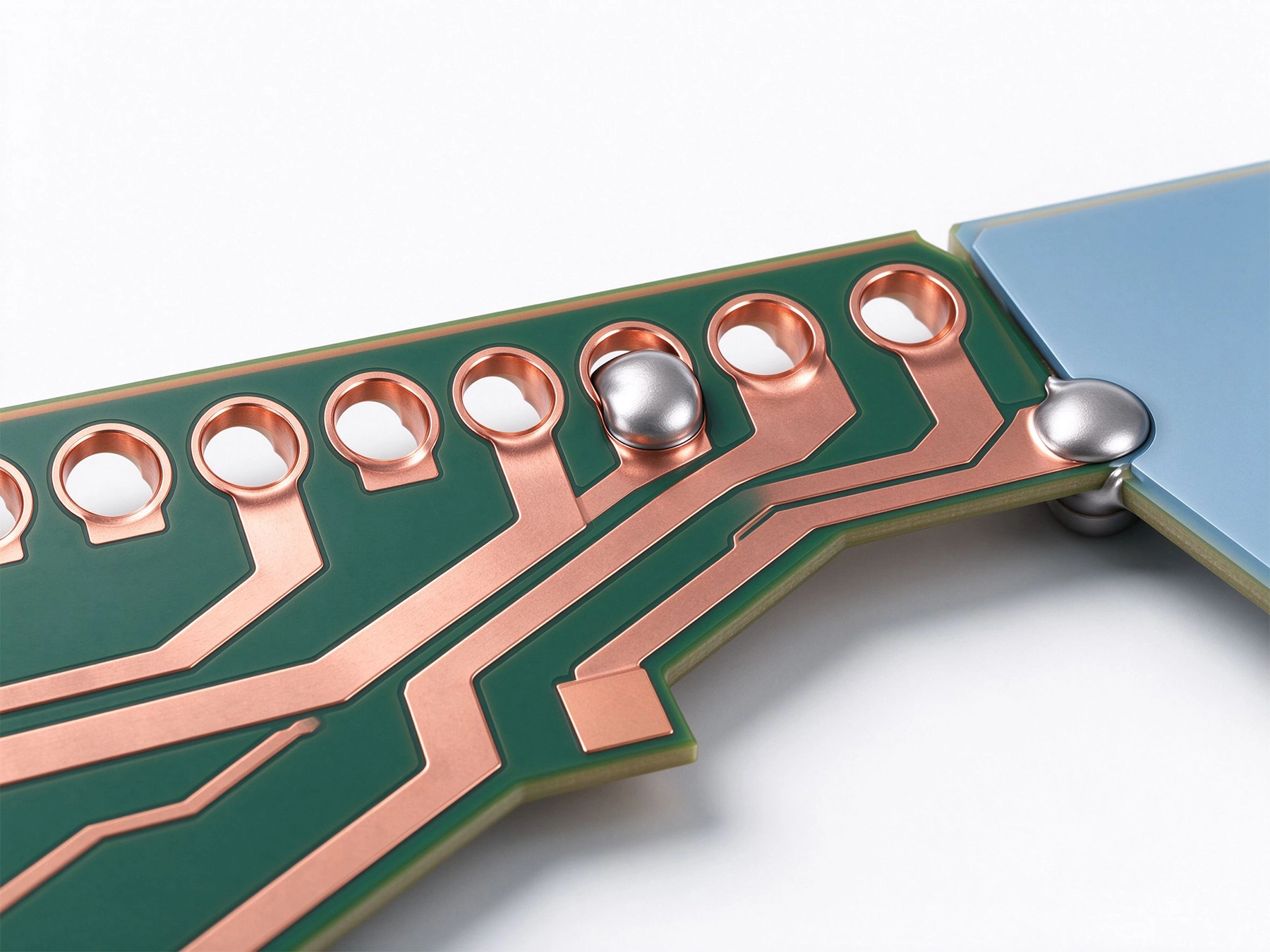
Castellated holes are formed by plating through-holes along the edge of a PCB, then cutting the board through the center of the holes during routing, leaving a series of half-moon shaped plated indentations along the board edge. This creates a surface-mountable edge connection that can be soldered directly to pads on a carrier board, eliminating the need for separate connectors or through-hole mounting.
In high-current applications, castellated holes offer several advantages over traditional connection methods. They provide a much lower profile than through-hole connectors, making them ideal for compact power modules where height is constrained. The distributed connection across multiple holes spreads current over a larger area, reducing resistance and improving Heat Dissipation compared to single-point connections. They also simplify assembly, as modules with castellated edges can be assembled using standard surface mount reflow processes rather than requiring separate Wave Soldering or hand assembly steps.
Common high-current applications for castellated holes include Battery Management System modules for electric vehicles, power supply modules for industrial equipment, motor driver boards for robotics, and charging modules for consumer electronics. In each of these applications, the castellated holes must carry tens or even hundreds of amps of current while maintaining reliable electrical and mechanical connections over thousands of thermal cycles.
The maximum current a castellated hole can carry safely depends on multiple design and manufacturing factors, all of which must be considered together to determine appropriate current ratings for your application. Relying on generic current rating tables designed for standard vias will almost always lead to under-designed connections that overheat under load.
Hole diameter and plating thickness are the most significant factors affecting current capacity. A larger hole provides more cross-sectional area for current flow, while thicker plating increases the effective conductive area of the hole wall. For high-current applications, a minimum hole diameter of 0.8mm is recommended, with plating thickness of at least 35 microns. For currents above 20 amps per hole, increase the hole diameter to 1.0mm or larger and specify plating thickness of 40 microns or more.
Copper Weight of the connected traces also affects current capacity. The traces feeding the castellated hole must have sufficient cross-sectional area to carry the same current as the hole itself. If the trace is narrower than required, it will become the bottleneck, overheating before the hole reaches its maximum current capacity. As a general rule, the trace width connected to each castellated hole should be sized to carry 120% of the current expected for that hole to provide an adequate safety margin.
Thermal dissipation characteristics determine how much heat the connection can shed during operation. Castellated holes connected to large copper planes will have higher current ratings than holes connected only to narrow traces, because the plane acts as a heat spreader that dissipates heat away from the connection. Holes on outer layers also dissipate heat better than internal castellated holes (if used), as they can radiate heat directly to the environment or to a heat sink attached to the board surface.
Number of parallel holes per connection significantly increases total current capacity. When multiple castellated holes are connected in parallel to carry a single High Current, the total current capacity is the sum of individual hole capacities minus a small derating factor to account for slight current imbalances between holes. For example, four 20-amp holes connected in parallel can safely carry approximately 70 to 75 amps total, rather than the full 80 amps, to account for small manufacturing variations that might cause uneven current sharing.
Solder Joint Reliability is the most common failure point for castellated hole connections under High Current loads. The unique geometry of the half-hole creates soldering challenges that standard surface mount pads do not face, and these challenges are amplified when the connection carries high currents that generate heat and cause Thermal Cycling.
Solder wetting inconsistency is the most frequent manufacturing issue with castellated holes. The curved surface of the half-hole makes it more difficult for solder to wet consistently across the entire plated surface compared to a flat pad. Poor wetting reduces the effective contact area between the hole and the carrier board pad, increasing resistance and leading to overheating under load. In severe cases, partial wetting can create high-resistance points that fail catastrophically under sustained current.
Thermal Cycling fatigue is the primary long-term failure mode for high-current castellated connections. Each time the current turns on and off, the connection heats up and cools down, causing expansion and contraction of the solder joint. Over time, this repeated stress causes crack formation in the solder, eventually leading to complete joint failure. The risk of fatigue failure increases with higher operating temperatures, larger temperature swings, and higher current loads.
Mechanical stress from board flex or vibration also affects Solder Joint Reliability. Castellated hole connections are often located along board edges, which are more prone to flex during handling or operation. Flexing creates mechanical stress in the solder joints that can cause cracks to form and propagate over time, especially when combined with thermal stress from high current operation.
Solder voiding is another common issue that reduces joint reliability. Voids form when outgassing from flux or surface contamination gets trapped in the solder during reflow. Voids reduce the effective contact area of the joint, increasing resistance and creating stress concentration points that accelerate fatigue failure. For high-current applications, voiding should be limited to less than 10% of the joint area to maintain acceptable reliability.
Following proven design rules for castellated holes minimizes the risk of both overheating and solder joint failure. These rules account for the unique geometry and manufacturing requirements of castellated connections in high-current applications.
Size holes appropriately for your current requirements. As a starting point, use the following guidelines for 35 micron plating thickness and 20°C maximum temperature rise: 0.6mm holes carry up to 10A per hole, 0.8mm holes carry up to 18A per hole, 1.0mm holes carry up to 25A per hole, and 1.2mm holes carry up to 32A per hole. Derate these values by 20% for high-temperature environments or applications requiring high reliability, and derate an additional 10% if holes are connected to inner layers only.
Specify sufficient plating thickness for both the hole walls and the cut edge. Standard plating thickness of 25 microns is insufficient for high-current applications, as the thin plating will overheat under load and may wear away during routing. Specify a minimum of 35 micron plating for holes carrying up to 20A, and 40 micron or heavier plating for higher current applications. Also specify that the cut edge of the castellated hole receives plating coverage, as exposed base copper on the cut edge can corrode over time and reduce joint reliability.
Design carrier board pads to extend beyond the edge of the module. The pad on the carrier board should extend 0.3mm to 0.5mm beyond the edge of the castellated module to provide a solder fillet that improves both mechanical strength and electrical contact. The pad width should match the length of the castellated hole along the board edge, and should include a mask relief of at least 0.1mm around the pad to prevent solder bridging between adjacent holes.
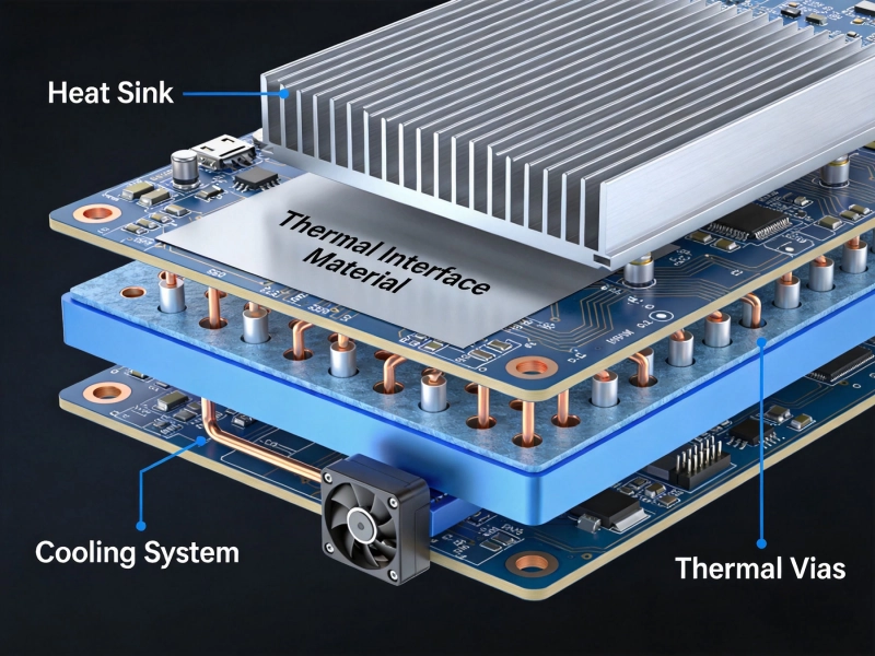
Include adequate thermal relief and heat spreading for each connection. Connect each castellated hole to a copper plane on at least one layer of the module board to spread heat away from the joint. If the module will be mounted to a heat sink, place Thermal Vias near the castellated holes to conduct heat away from the connection and into the heat sink. Avoid placing high-power components near the castellated edge, as their additional heat will raise the operating temperature of the connections.
Space adjacent holes appropriately to prevent solder bridging and electrical arcing. For high-current applications, maintain a minimum of 0.5mm spacing between adjacent castellated holes for voltages below 50V, and increase spacing to 1.0mm or more for higher voltage applications. This provides sufficient room for solder fillets without risk of bridging, and meets minimum Creepage And Clearance requirements for your voltage class.
Even the best design will fail if manufacturing processes are not properly controlled. Working with your manufacturer to implement the following process controls ensures consistent, reliable castellated hole connections for high-current applications.
Routing sequence and tool selection affect the quality of the castellated edge. Castellated holes should be drilled first, then fully plated, before the board edge is routed. Use a sharp routing bit with appropriate feed and speed settings to minimize burr formation and ensure a clean cut through the center of the holes. Dull bits cause rough cuts that leave copper burrs along the edge, which can cause solder bridging or poor wetting during assembly.
Edge plating process control is critical for long-term reliability. After routing, the exposed copper on the cut edge of the holes must be cleaned and plated to prevent corrosion and improve solderability. Some manufacturers use a secondary plating process specifically for the cut edge, while others optimize the initial plating process to ensure coverage on the edge surfaces. Verify that your manufacturer has experience with edge-plated castellated holes and can demonstrate consistent plating coverage on the cut edge.
Solder paste application requires stencil design adjustments for castellated connections. Use a stencil thickness of 0.15mm to 0.2mm for castellated hole joints, and slightly increase the paste volume for these pads compared to standard surface mount pads. The extra paste ensures sufficient solder to fill the half-hole cavity and form a strong fillet along the edge of the module. For high-current applications, consider using a stepped stencil to provide even more paste volume for the castellated connections without risking solder bridging on finer pitch components.
Reflow profile development should account for the higher thermal mass of castellated connections. The large copper area of the holes and connected planes may require a longer soak time or slightly higher peak temperature to ensure proper solder wetting on both the hole surface and the carrier pad. Use thermocouples attached to actual castellated joints during profile development to verify that the solder reaches the required melting temperature and flows properly across the entire connection area.
Validating the current rating and solder reliability of your castellated hole design before volume production prevents field failures and expensive redesigns. The following tests provide the data needed to confirm your design meets performance and reliability requirements.
Current Carrying Capacity testing verifies the maximum current the connection can handle without exceeding your temperature rise limit. This test involves passing increasing levels of current through the connection while monitoring the temperature with thermocouples, until the desired temperature rise is reached. Perform this test on multiple sample boards to account for manufacturing variations, and apply a 20% derating factor to the measured maximum current to determine the rated current for production designs.
Thermal cycle testing validates long-term solder joint reliability under repeated temperature swings. Typical test conditions involve cycling between -40°C and 125°C for 500 to 1,000 cycles, with resistance measurements taken periodically throughout the test to detect joint degradation. A significant increase in resistance during testing indicates joint cracking or failure, and requires design or process adjustments to improve reliability.
Shear strength testing measures the mechanical strength of the solder joint. This test applies force to the edge of the module until the connection breaks, measuring the force required to separate the module from the carrier board. For high-current applications, the minimum shear strength per hole should be at least 50N, with failure occurring in the solder rather than at the copper-plated interface or in the substrate material. Lower strength indicates poor solder wetting or insufficient plating adhesion that will lead to reliability problems in the field.
Cross-section analysis of solder joints reveals internal defects that are not visible from the outside. Cut and polish sample joints to examine the solder fillet shape, wetting coverage, and void percentage. Solder should wet at least 75% of the castellated hole surface, and voids should make up less than 10% of the total joint area for high reliability. Cross-sectioning also verifies plating thickness and coverage on both the hole wall and the cut edge.
Even with careful design and manufacturing, castellated hole connections can fail if unexpected issues arise. Understanding these common failure modes and how to prevent them helps you address potential problems before they lead to field failures.
Overheating failure occurs when the current exceeds the connection's capacity, causing the solder to melt or the plating to delaminate. Prevention involves correctly sizing holes for your current requirements, providing adequate heat spreading, and derating connections appropriately for the operating environment. Monitoring connection temperatures during prototype testing confirms your design can handle the expected current without excessive temperature rise.
Solder joint fatigue failure from thermal cycling is the most common long-term failure mode. Prevention includes using sufficient solder volume to form a strong fillet, reducing operating temperature ranges where possible, and using high-tin solder alloys with good fatigue resistance. For extremely harsh environments, consider adding mechanical reinforcement such as adhesive or mounting brackets to reduce stress on the solder joints.
Corrosion failure occurs when exposed copper on the cut edge is not properly plated or protected. Prevention involves specifying edge plating for the castellated holes, using appropriate surface finishes, and ensuring the final assembly includes conformal coating if the product will operate in high-humidity or corrosive environments. Avoid using castellated holes in applications where they will be directly exposed to moisture or chemicals without adequate protection.
Solder bridging between adjacent holes causes short circuits that can destroy both the module and the carrier board. Prevention involves maintaining adequate spacing between holes, using appropriate solder paste volumes, and optimizing the reflow profile to prevent excessive solder flow. Including test points for continuity testing after assembly allows you to catch any bridging issues before products leave the factory.
Castellated holes offer a compact, cost-effective connection solution for High-current Pcb modules, but their current rating and solder reliability require careful attention to design, manufacturing, and testing details. Understanding the factors that affect current capacity, the challenges of soldering half-hole geometries, and the proven design rules for reliable operation allows you to take full advantage of castellated connections without sacrificing performance or long-term reliability.
The most successful castellated hole designs combine appropriately sized holes with sufficient plating thickness, well-designed carrier board pads, adequate thermal spreading, and validated manufacturing processes. Testing current capacity, thermal cycling reliability, and joint strength during prototype development confirms your design meets requirements before volume production begins, reducing the risk of expensive field failures later.
As demand for compact high-Power Electronics continues to grow in electric vehicles, industrial equipment, and consumer electronics, castellated holes will become an increasingly common connection method. Building your expertise in designing and manufacturing reliable high-current castellated connections now positions you to meet these demands effectively as they become more prevalent across industries.
Contact us to discuss your requirements and explore how high-current castellated hole design and manufacturing capabilities can support your product development.
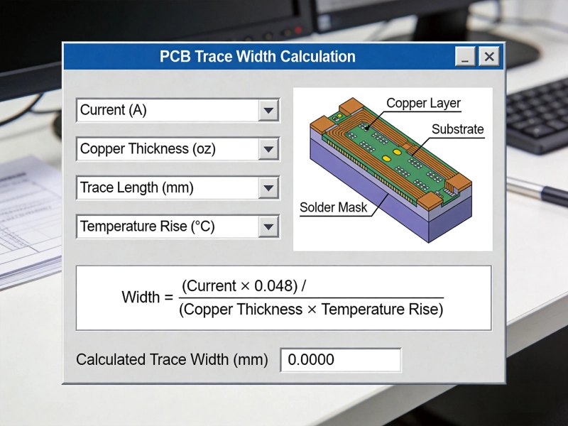
High Current PCB Trace Width Calculator: Complete Guide with Formulas and ExamplesMay/20/2026
High Current PCB Copper Fill: Solid Pour vs. Hatched Pattern PerformanceSeptember/17/2026
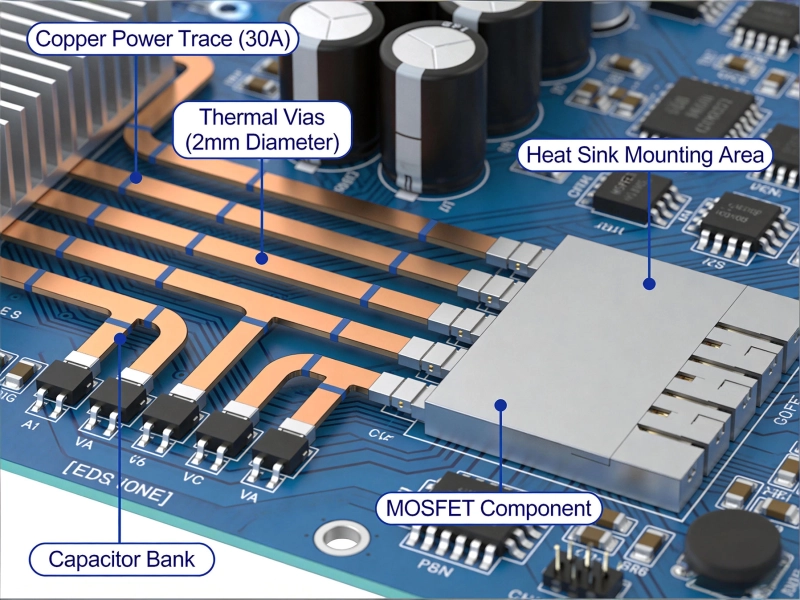
How to Design High Current PCB Traces: A Complete GuideMay/20/2026
High Current PCB Copper Balancing: Preventing Warpage in Heavy Copper BoardsSeptember/07/2026

High Current PCB EMI Shielding: Ground Pour vs. Shielding CansAugust/14/2026
High Current PCB Material Showdown: FR4 vs. Metal-Core vs. PolyimideJuly/14/2026
How to Reduce Temperature Rise in Power PCBJune/17/2026

High Current PCB Design for High-Power Laser SystemsOctober/22/2026