

Heavy Copper PCBs power everything from Electric Vehicle chargers to Industrial Motor Drives, carrying currents that would destroy standard circuit boards. Yet the very copper that makes these boards capable of handling high amperage also creates one of the most persistent manufacturing challenges: warpage. When thermal expansion during lamination pulls unevenly on the board structure, the result ranges from minor bow that complicates assembly to severe twist that renders boards completely unusable. Understanding copper balancing helps you design Heavy Copper boards that manufacturers can produce reliably.
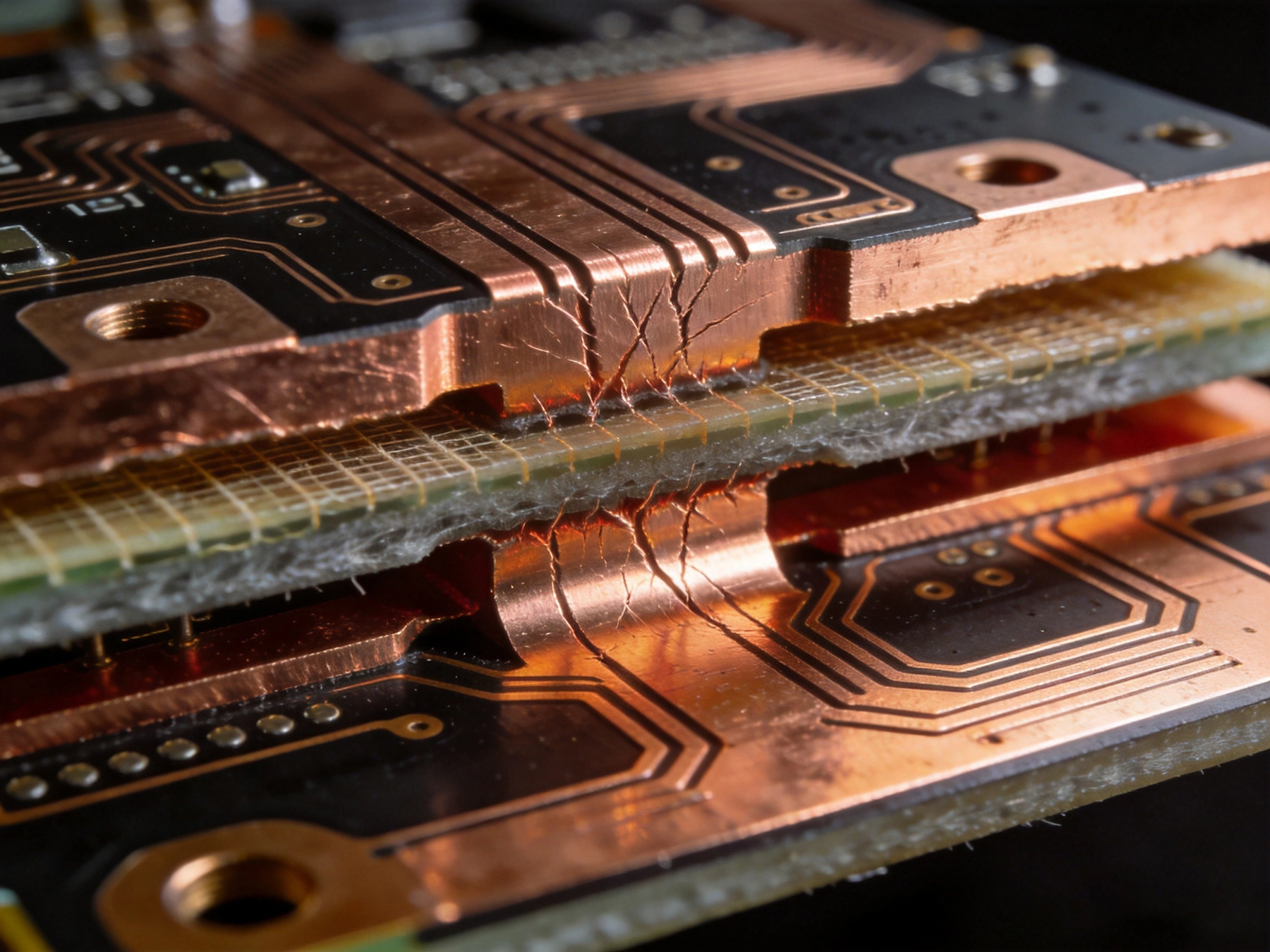
Standard PCB copper is typically 1 ounce per square foot, equal to about 35 micrometers thickness. Heavy copper boards start at 2 or 3 ounces and go up from there. Some designs use 6 ounces, 10 ounces, or even thicker copper for bus bars and Power Distribution. The physical mass of copper changes everything about how the board behaves during manufacturing.
Copper has a thermal expansion coefficient roughly five times higher than the FR4 substrate material that surrounds it. When the board heats up during lamination or subsequent assembly processes, the copper wants to expand more than the substrate. In a balanced board where copper distribution is even across all layers, these forces cancel out. In an unbalanced board, the layers with more copper expand more, creating internal stress that bends the entire structure.
Heavy copper also affects how heat moves through the board. Power Electronics generate significant heat that must flow through copper planes to Thermal Vias and Heat Sinks. If copper distribution is uneven, some areas conduct heat better than others, creating temperature gradients that worsen warpage during operation.
Copper balancing means ensuring that the total copper area on each layer of a multilayer board is approximately equal. This does not mean every layer must have the same pattern. A ground plane layer naturally has more copper than a signal routing layer, but the overall copper coverage percentage should stay within tight tolerances across all layers.
The typical target is keeping copper coverage between 40% and 60% on each layer. Some manufacturers accept as low as 30% with compensation techniques, while others recommend adding copper thieving or non-functional pads to reach minimum coverage. Going above 80% creates problems with etching and plating, so staying in the 40-60% sweet spot simplifies manufacturing.
Balance is measured as the ratio between the layer with the most copper and the layer with the least. A 1:1 ratio is ideal, meaning all layers have equal copper coverage. In practice, ratios up to about 1.3:1 are manageable. Beyond 1.5:1, warpage risk increases significantly and manufacturing costs rise due to special handling requirements.
The lamination process applies heat and pressure to bond all layers together. During this process, the board temperature exceeds 170 degrees Celsius, well above the glass transition temperature of the substrate. The material softens and flows around the copper features, then hardens as it cools. If one side of the board has more copper than the other, it resists cooling contraction more than the opposite side.
Imagine a six-layer board where layers two and five are solid copper Power Planes while layers three and four are signal routing with only 20% copper coverage. During lamination, the solid planes want to stay expanded because of their thermal mass. The thin signal layers have less resistance to movement. The board twists as it cools because one side of the structure has more copper pulling inward than the other.
The problem compounds through subsequent manufacturing steps. Solder reflow exposes the board to temperatures above 250 degrees Celsius for lead-free assembly. Each thermal cycle adds stress that can increase warpage. Boards that pass dimensional inspection after lamination may fail after assembly if thermal profiles are aggressive.
The most reliable heavy copper designs use completely symmetric stackups. If layer one has three ounces of copper, layer six should also have three ounces. If layer two has two ounces, layer five should match. This mirror symmetry means thermal expansion forces act equally on both sides of the board centerline.
For odd-layer boards like five-layer or seven-layer stacks, achieving perfect symmetry requires adding a layer or using dummy copper to balance the center layer against a combination of outer layers. A five-layer board with a heavy copper core might have the core layer as a four-ounce plane, the two inner layers as two-ounce routing, and the two outer layers as one-ounce surfaces. The distribution balances even though individual layers differ.
Copper thieving, also called copper flooding or non-functional land, adds copper to areas of a layer that would otherwise have little or no copper. These features are electrically isolated from the circuit and exist purely for manufacturing purposes. They increase copper coverage without affecting circuit function.
Thieving patterns typically use small isolated squares or crosshatch patterns placed between routing and pads. The features should be electrically isolated with no connection to any net. Many manufacturers provide guidelines for minimum thieving size and maximum spacing. Some require thieving to be clearly marked in documentation so they are not confused with intentional features.
Using crosshatched copper planes instead of solid planes reduces copper coverage while maintaining most of the electrical benefits. A 50% hatched ground plane provides nearly equivalent impedance and Current Distribution compared to a solid plane, while significantly improving copper balance with routing layers.
The trade-off involves impedance control and current handling. Solid planes provide consistent reference impedance, while hatched planes have slightly higher impedance variation. For Power Distribution, hatched planes handle current well but may have higher resistance due to reduced cross-sectional area. Evaluate whether your design requirements justify the complexity of hatching versus adding thieving to balance solid planes.
Modern Pcb Design software includes tools for analyzing copper coverage on each layer. In Altium Designer, the Property Panel shows coverage percentage for each layer when you run a coverage report. In Cadence Allegro, the Analyze menu provides coverage calculations. Even simple tools likegerber viewers can estimate coverage by analyzing the ratio of copper area to total board area.
When calculating coverage, include all copper features: traces, pads, vias, plane areas, and any copper thieving you have added. Most design tools calculate total copper area directly. Compare the coverage percentages across all layers and note any that fall below your target threshold.
If your signal layers have low coverage due to sparse routing, consider adding ground fills or copper thieving to bring them closer to balance. This is especially important for inner layers adjacent to heavy copper planes. The contrast between a solid plane layer and an empty routing layer creates the most stress concentration.
Heavy copper boards often use smaller panels than standard boards to manage warpage during processing. A board with four-ounce copper on multiple layers may need to be produced in smaller arrays to keep dimensions stable through plating and lamination steps. Discuss panel size limitations with your manufacturer early in the design phase.
Mouse bite or V-score panelization affects how stress distributes through the array. Boards with significant imbalance may require additional margin around the panelization features or use of breakaway tabs instead of scores. Your manufacturer can recommend panelization approaches that work with your balance constraints.
Experienced heavy copper manufacturers adjust lamination parameters based on copper distribution. Higher pressure can help压 (press) copper more evenly into the substrate, reducing stress gradients. Slower cooling rates allow more gradual contraction that minimizes warp. These process adjustments add cost and lead time but often eliminate the need for design changes.
Ask your manufacturer what their standard process parameters are for heavy copper and whether they customize for unbalanced designs. Some manufacturers have proprietary techniques for managing warpage that do not require design modifications. Understanding these capabilities helps you decide whether to optimize your design or rely on manufacturing process control.
Manufacturers inspect finished boards for warpage using backlighting techniques or coordinate measuring machines. Backlight inspection passes light through the board and measures how much bends between the light source and camera. IPC standards define maximum warpage limits based on board size and application.
For boards that must pass strict flatness requirements, specify warpage limits explicitly in your procurement documentation. Standard IPC Class 2 and Class 3 accept certain warpage levels that may be unacceptable for your application, especially if the board mounts to a flat heatsink or undergoes automated assembly.
Heavy copper serves two purposes in Power Electronics: conducting High Current and dissipating heat. The copper cross-sectional area determines current capacity according to Ipc-2152 standards or manufacturer derating curves. A two-ounce trace carries significantly more current than a one-ounce trace of the same width because of reduced resistance and improved heat spreading.
Thermal Vias through power pads connect top-layer copper to internal planes for heat removal. The number and size of thermal vias affects how effectively heat transfers to the internal planes. If internal planes are imbalanced, some areas remove heat better than others, creating temperature gradients that contribute to operational warpage.
Consider using spreader bars or copper coin attachments for extreme current applications. These heavy copper features attach to the board surface and handle most of the current, but they introduce significant imbalance that requires careful management on adjacent layers.
Provide your manufacturer with copper coverage analysis before releasing your design. Highlight any layers with coverage below your target threshold. Ask whether they recommend design changes or can accommodate the imbalance through process adjustments. Many manufacturers offer DFM analysis that specifically checks for warpage risk factors.
If your design has unavoidable imbalance due to functional requirements, discuss this with your manufacturer upfront. Some designs genuinely require asymmetric copper distribution, and experienced heavy copper manufacturers have developed techniques to manage these cases. They may recommend specific layer ordering, alternative substrate materials, or special pressing sequences that reduce warp despite the imbalance.
Substrate materials with higher glass transition temperatures (Tg) resist warpage better than standard FR4. High-Tg materials like Tg 170 or Tg 150 maintain stiffness at higher temperatures, reducing how much the board deforms during lamination cooling. For severe heavy copper applications, consider using resin systems specifically formulated for power electronics.
Low-flow prepregs reduce void risk in heavy copper designs but may not fill gaps between large copper features adequately. High-flow prepregs fill gaps well but may squeeze out excessive resin during pressing. Your manufacturer selects prepreg based on the copper geometry of your specific design.
Some manufacturers offer resin filled and pressed (RFP) via technology for heavy copper designs. This process fills via barrels with resin before lamination, creating a smoother surface and better filling of gaps between heavy copper features. The result is more consistent copper-to-resin ratio across the board.
Request warpage measurement data on first article boards before approving production. The manufacturer should measure boards at room temperature and after simulated reflow exposure to verify that warpage remains within limits through the assembly process. Document the results and establish baseline expectations for production.
For critical applications, consider performing Thermal Cycling tests that measure warpage at temperature extremes. Boards may appear flat at room temperature but warp significantly when heated. If your board operates in a thermal environment, its behavior at temperature matters more than its room temperature flatness.
Adding copper thieving after routing is complete often creates DRC violations or accidentally connects to signal nets. Plan copper balancing from the beginning of layout, or use dedicated thieving layers that are clearly separated from signal routing.
Assuming that external layers do not need balance because components mount on them is a serious error. Outer layers experience the same thermal forces during lamination and assembly. An unbalanced outer layer causes as much warpage as an internal imbalance.
Relying solely on manufacturing process control without addressing design imbalance increases cost and risk. Process adjustments have limits, and boards with extreme imbalance may require multiple pressing cycles or special fixtures that add significant expense. Designing for balance is always preferable to compensating in manufacturing.
Copper balancing is essential for producing flat, reliable heavy copper boards. The thermal expansion mismatch between copper and substrate creates stress during manufacturing and assembly that causes warpage in unbalanced designs.
Design for 40-60% copper coverage on all layers with coverage ratios no greater than 1.3:1 between the heaviest and lightest layers. Use symmetric stackups whenever possible. Add copper thieving to layers that cannot achieve adequate coverage through routing.
Work with your manufacturer early to understand their capabilities and limitations for heavy copper. Provide copper coverage analysis in your design documentation and discuss any unavoidable imbalances before releasing for production.
Specify warpage limits explicitly in your procurement documentation and request first article measurement data. Validate that boards remain flat through simulated assembly thermal exposure, not just at room temperature.
By designing with balance in mind, you create heavy copper boards that are manufacturable at reasonable cost and reliable in service.
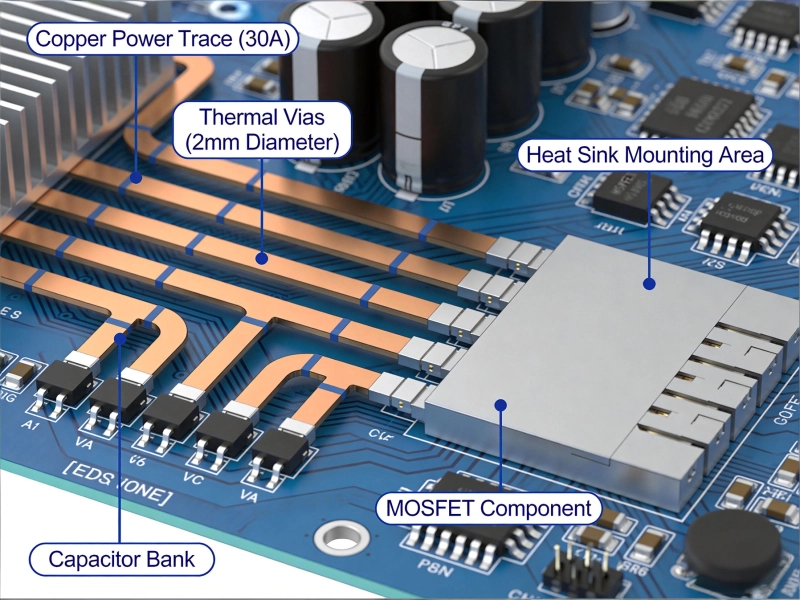
How to Design High Current PCB Traces: A Complete GuideMay/20/2026
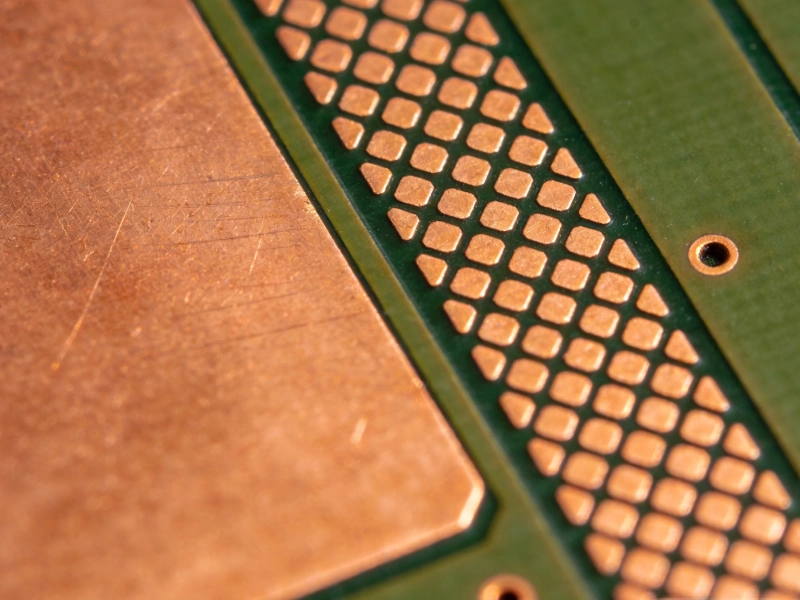
High Current PCB Copper Fill: Solid Pour vs. Hatched Pattern PerformanceSeptember/17/2026
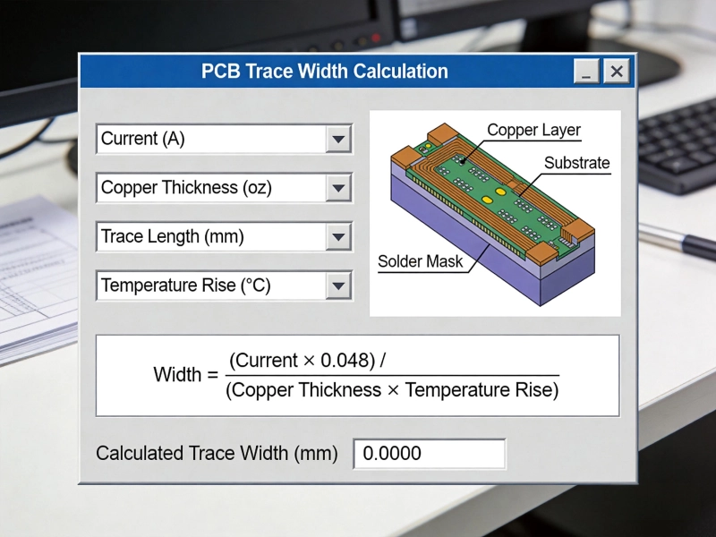
High Current PCB Trace Width Calculator: Complete Guide with Formulas and ExamplesMay/20/2026
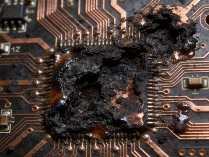
High Current PCB Failure Modes and PreventionJune/18/2026
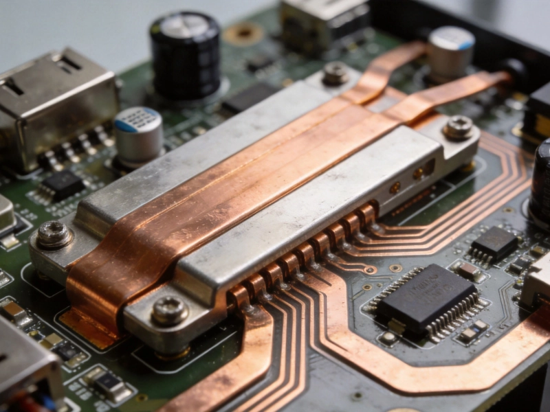
High Current PCB Design for Electric Vehicle Charging StationsAugust/15/2026
High Current PCB Design for Data Center Power ShelvesOctober/19/2026
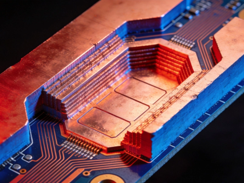
High Current PCB Embedded Copper: Internal vs. External Heat DissipationSeptember/26/2026
High Current PCB Routing: 45-Degree Angles vs. Curved Traces in PracticeJuly/12/2026