High-power laser systems used in industrial cutting, medical surgery, scientific research, and defense applications rely on stable, efficient power delivery to deliver consistent performance. These systems often require PCB designs that can carry 50A to 200A of continuous current, with peak pulse currents exceeding 300A for short durations. Poorly designed High Current PCBs for laser systems can lead to excessive voltage drops, overheating, component failure, or even catastrophic thermal runaway that damages the entire laser system. Following proven High Current Design principles is critical to ensuring your laser system operates reliably over its intended lifecycle.

Unique High Current Design Challenges for Laser Systems
Laser systems present specific design challenges that differ from standard high power electronic products:
- Extreme Current Density requirements: Diode-pumped solid-state lasers, fiber lasers, and CO2 laser drivers often require 12V to 48V supplies delivering 50A to 200A of continuous current, with pulse currents 2-3x higher during laser firing events.
- Tight voltage regulation requirements: Laser diode output power is extremely sensitive to input voltage; even a 0.5V drop in the supply path can reduce laser output power by 10% or more, leading to inconsistent performance in industrial or medical applications.
- Thermal sensitivity: Excess heat from High Current paths can drift laser diode wavelength, reduce efficiency, and shorten component lifespan. Most high-power laser systems require component operating temperatures to stay within ±2°C of setpoint for optimal performance.
- Emi susceptibility: High current switching in laser drivers generates significant electromagnetic interference that can disrupt sensitive laser control circuits, temperature sensors, and feedback loops if not properly contained.
- Safety requirements: Fault conditions in high current paths can cause fires, electrical arcs, or damage to expensive laser diodes that cost thousands of dollars to replace.
Core High Current PCB Design Guidelines for Laser Systems
Follow these proven design principles to build reliable, high-performance PCBs for high-power laser systems:
1. Current Carrying Path Optimization
The most critical aspect of High Current PCB design is ensuring the current carrying paths can handle the required load without excessive voltage drop or heating:
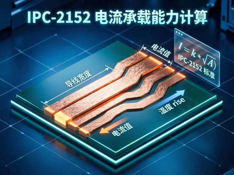
- Calculate trace width with appropriate safety margins: Use Ipc-2152 standards for Trace Current Capacity, not outdated online calculators that overestimate current carrying capability. For example, a 1oz (35µm) Copper Trace can safely carry approximately 10A with a 10°C temperature rise when 4mm wide. For 50A continuous current, you need a 22mm wide 1oz trace, or an 11mm wide 2oz trace. Always add 20-30% extra width as a safety margin for unexpected load conditions.
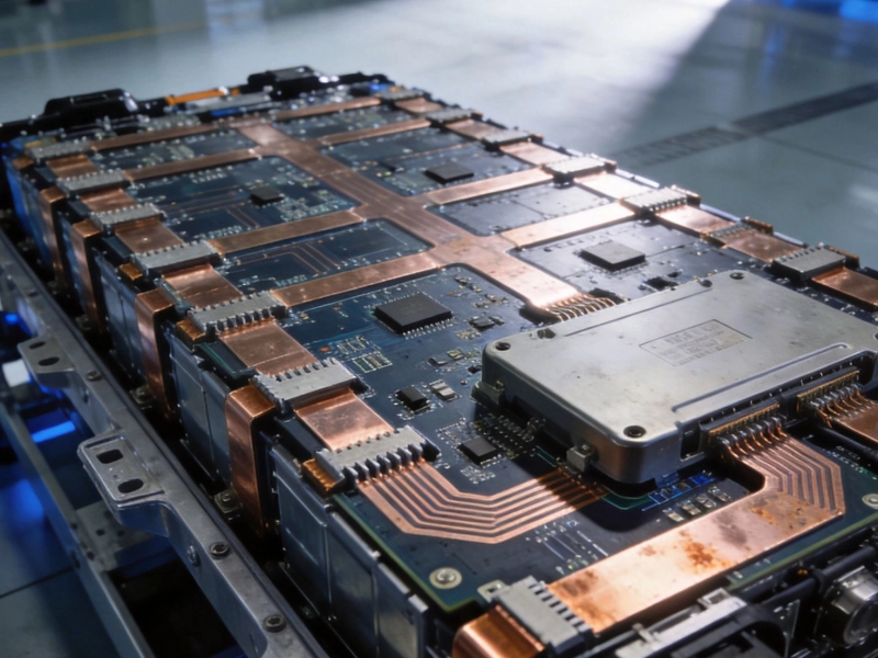
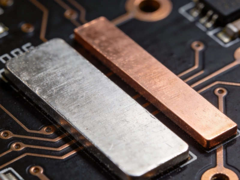
- Use thick copper foils for high current paths: For laser systems carrying more than 30A, use 2oz (70µm) or 4oz (140µm) copper foils for power layers. Thick copper reduces trace resistance, lowers I²R losses, and improves Heat Dissipation. For currents above 100A, consider Heavy Copper PCBs with 6oz to 10oz copper layers.
- Avoid current bottlenecks: Never reduce trace width in high current paths unless absolutely necessary. Even a short narrow section of trace can create a hot spot that leads to failure. Ensure all connectors, vias, and component pads are rated for the full current load.
- Design vias correctly for high current: Standard 0.8mm diameter plated vias with 1oz copper can carry approximately 5A of continuous current. For a 50A path, you need at least 12 vias (10 for current carrying plus 20% margin) in parallel to avoid via overheating. Place vias evenly across the current path to ensure even Current Distribution, and avoid stacking vias that can restrict flow.
- Use dedicated Power Planes: For currents above 20A, use full copper layers for positive supply and ground returns instead of individual traces. Planes offer lower resistance, better heat distribution, and reduced Emi compared to discrete traces. Ensure Power Planes are continuous with no slots or cutouts that would force current to take long, high-resistance paths.
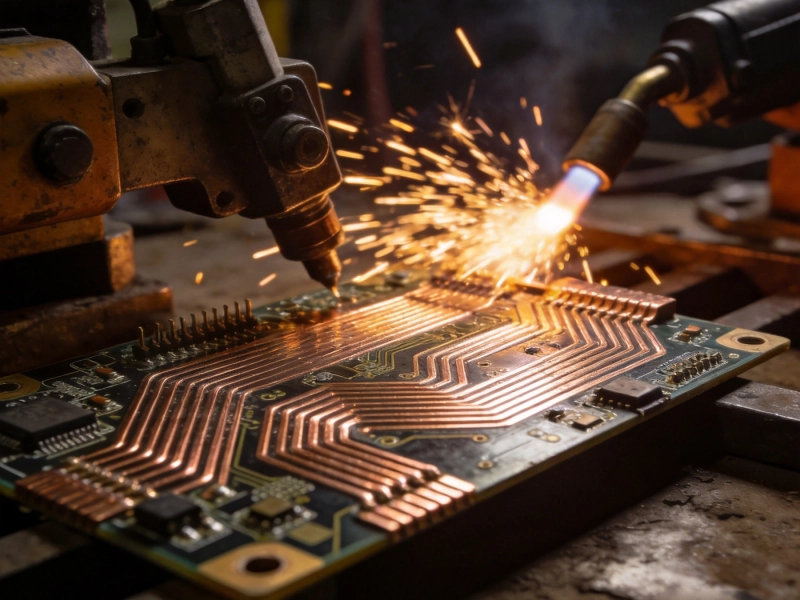
- Apply solder to high current traces: Leave high current traces uncovered by solder mask, and apply additional solder during assembly to increase effective Copper Thickness by 50-100%, boosting Current Carrying Capacity without increasing trace width.
2. Thermal Management Design
Even with correctly sized traces, high current paths generate significant heat that must be dissipated to maintain laser performance and reliability:
- Place high power components strategically: Position laser diodes, power MOSFETs, and current sensing resistors near the edges of the PCB where they can be directly mounted to external Heat Sinks or the system chassis. Group high power components together to simplify Thermal Management, but avoid clustering them so tightly that heat builds up in a single area.
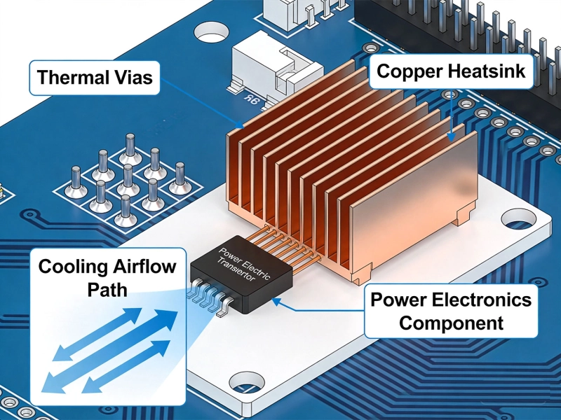
- Use Thermal Vias under high power components: Place an array of 0.5mm Thermal Vias under power MOSFETs and laser diode packages to conduct heat from the top layer to internal ground planes or bottom layer Heat Sinks. Use 8-12 vias per high power component, spaced 1mm apart for optimal heat transfer.
- Select appropriate PCB materials: For laser systems operating at power levels above 100W, use high-Tg FR-4 material (Tg ≥ 170°C) instead of standard FR-4 to withstand higher operating temperatures. For systems above 500W, consider metal core PCBs (MCPCB) with aluminum or copper bases that offer 5-10x better thermal conductivity than FR-4. For extreme temperature environments, use aluminum nitride or alumina Ceramic Substrates that offer superior thermal performance and electrical isolation.
- Include temperature monitoring points: Place NTC thermistors or thermocouple pads near high current paths and laser diode packages to allow real-time temperature monitoring during operation. Implement over-temperature protection circuits that reduce laser power or shut down the system if temperatures exceed safe limits.
- Optimize airflow over the PCB: Design the Pcb Layout to align with the system's airflow path, ensuring high power components receive direct cooling. Avoid placing tall components upstream that would block airflow to heat-sensitive laser components.
3. Grounding and EMI Mitigation
High current switching in laser drivers creates significant electrical noise that can disrupt sensitive control circuits if not properly managed:
- Separate power and signal grounds: Use a star grounding topology where high current power grounds and low-level signal grounds connect at a single point, preventing high current return paths from injecting noise into sensitive control circuits. Never route high current return paths near temperature sensors, laser feedback circuits, or communication interfaces.
- Minimize current Loop Area: Route high current supply and return paths as close together as possible to minimize the Loop Area, which reduces radiated EMI by up to 90%. For discrete traces, keep supply and return traces parallel and separated by no more than 0.5mm. For plane layers, use adjacent power and ground planes to create a low-inductance path.
- Add transient suppression components: Place TVS diodes directly across laser diode power inputs to clamp voltage spikes from inductive switching events. Use bulk electrolytic capacitors and high-frequency ceramic capacitors near power MOSFETs to stabilize supply voltage during high current pulse events.
- Shield sensitive circuits: Use copper shield planes around laser feedback circuits and temperature sensing paths to isolate them from high current noise. Connect shield planes to ground at a single point to avoid creating ground loops.
4. Component and Connector Selection
Even the best Pcb Layout will fail if components are not rated for the required current:
- Oversize current carrying components: Select power MOSFETs, shunt resistors, and fuses with current ratings at least 50% higher than your maximum expected load. For laser systems with high pulse currents, ensure components are rated for the peak pulse current as well as continuous current.
- Use high current connectors: Select connectors with gold-plated contacts rated for at least 125% of your maximum current. For currents above 30A, use crimped connections instead of soldered connections for higher reliability. Avoid using standard 0.1" header connectors for high current paths, as they are typically only rated for 1-3A per pin.
- Select appropriate soldering materials: Use high-temperature solder (SAC305 or higher) for high current connections to avoid solder joint fatigue from Thermal Cycling. For extremely high current applications, use pressure-fit terminals instead of soldered connections for improved reliability.
Common High Current Design Mistakes to Avoid
Even experienced designers often make these avoidable mistakes when designing high current PCBs for laser systems:
- Ignoring pulse current requirements: Many designers calculate trace width based only on average current, forgetting that laser pulse currents can be 2-3x higher than average. Always size traces and components for peak current, not just average current.
- Insufficient via count: A common failure point is using too few vias to connect high current layers, leading to via overheating and eventual failure. Always calculate the required number of vias based on per-Via Current Capacity, and add a 20% safety margin.
- Neglecting return path design: Focusing only on the positive supply path while ignoring the Ground Return Path is a frequent mistake. The return path has the same current flow as the supply path and requires the same Current Carrying Capacity.
- Overlooking voltage drop: A 0.2V drop across a 50A path represents 10W of wasted power that turns into heat, plus a potential loss of laser output power. Measure voltage drop across high current paths during testing, and adjust trace width if drop exceeds 1% of supply voltage.
- Poor thermal coupling: Mounting high power components to the PCB without proper thermal vias or thermal interface material leads to heat buildup and premature component failure, even if the traces are correctly sized.
Case Study: 500W Fiber Laser Driver PCB
We recently designed a High Current PCB for a 500W industrial fiber laser system that required 80A continuous current with 180A peak pulse current. The design incorporated these key features:
- 4oz copper layers for power paths, with 28mm wide traces for main current carrying paths
- 16 parallel vias at each layer transition to handle the 80A continuous current
- Aluminum Metal Core Pcb base for improved thermal dissipation
- Thermal via arrays under power MOSFETs and laser diode packages
- Separated power and signal grounds with star grounding topology
- Adjacent power and ground planes to minimize loop area and EMI
During testing, the PCB showed a maximum voltage drop of just 0.12V across the entire current path at full load, with a maximum operating temperature of 61°C under continuous operation—18°C lower than the client's previous design. The system has now completed 12,000 hours of continuous operation without any failures.
Testing and Validation Requirements
Always validate your High Current Pcb Design before full production:
- Current load testing: Run the board at 125% of maximum rated current for 24 hours, monitoring temperature and voltage drop across all high current paths.
- Thermal imaging: Use an infrared thermal camera to identify hot spots during full load operation, paying special attention to vias, connector pins, and component solder joints.
- Pulse load testing: Test the board under actual laser pulse conditions to ensure it can handle peak currents without excessive voltage drop or overheating.
- EMI testing: Perform radiated and conducted EMI testing to ensure the design meets applicable standards for your industry, especially for medical or industrial laser systems.
- Thermal Cycling: Run 100+ temperature cycles from -10°C to 60°C to identify any solder joint or via reliability issues.
High Current Pcb Design for laser systems requires careful attention to current carrying capacity, Thermal Management, and Emi Mitigation to ensure reliable long-term performance. By following these guidelines, you can create robust designs that deliver consistent laser performance even under the most demanding operating conditions.
Contact us to discuss your requirements.