

In Power Electronics Pcb design, how you fill unused board area with copper matters more than most engineers realize. The choice between a solid Copper Pour and a hatched (crosshatch) copper pattern is not purely aesthetic—it directly impacts Current Carrying Capacity, thermal dissipation, Emi Shielding effectiveness, board warpage, and manufacturing yield. For High Current PCBs carrying tens or even hundreds of amps, this decision can mean the difference between a board that runs cool and stable and one that warps, delaminates, or fails prematurly under Thermal Cycling. This article examines both approaches in depth, comparing their real-world performance across the parameters that matter most in Power Electronics Design.
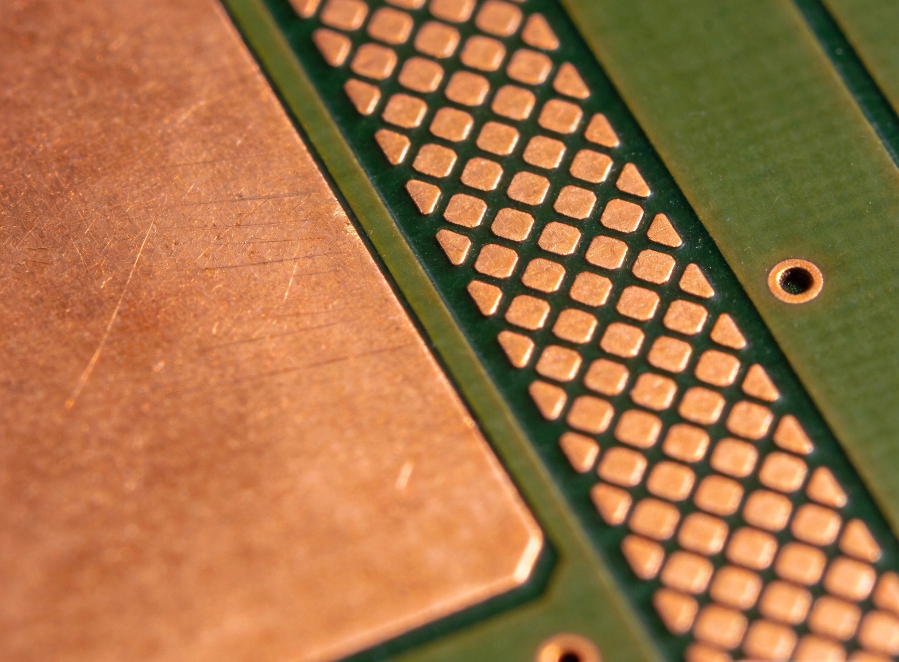
A solid Copper Pour fills every available square millimeter of a designated area with continuous copper. On inner layers, it typically serves as a power or ground plane. On outer layers, it provides a ground plane, Current Return Path, thermal spreading surface, or EMI shield. The pour is connected to the target net through thermal reliefs or direct connections at pads and vias.
The defining characteristic of a solid pour is its uninterrupted copper area. There are no gaps, no crosshatch lines, no removed copper—just a continuous sheet of conductor. This continuity is the source of its strengths and, paradoxically, some of its weaknesses in High Current applications.
A hatched copper fill replaces the continuous pour with a grid pattern of parallel copper traces at a specified spacing and orientation, typically with a second set of traces at 90° (or 45°) to create a crosshatch. The key parameters defining a hatched fill are:
The hatched pattern intentionally leaves gaps in the copper fill. These gaps are what give it its unique properties—both advantages and limitations—compared to a solid pour.
For high current PCBs, Current Carrying Capacity is often the primary design driver. At first glance, the comparison seems straightforward: solid copper has more copper, therefore it carries more current. The reality is more nuanced.
A solid copper pour provides the maximum possible cross-sectional area for current flow. For a 1 oz (35 μm) copper layer on a 100 mm wide pour, the available cross-section is 3.5 mm²—capable of carrying approximately 10–15A continuously depending on acceptable temperature rise, per Ipc-2152 calculations.
However, current in a solid pour does not distribute uniformly. High-frequency currents concentrate at the edges of the pour due to the skin effect, and DC currents tend to follow the shortest path between source and load. This non-uniform distribution means that even in a solid pour, only a portion of the available copper actively carries significant current, particularly for localized connection points.
A hatched fill with 50% copper coverage has, by definition, roughly half the cross-sectional area of a solid pour. If current capacity were purely proportional to cross-section, a 50% hatched fill would carry 50% of the current. In practice, the reduction is somewhat less severe because the hatch traces provide defined current paths that can distribute current more evenly than the non-uniform distribution in a solid pour.
For high current applications where the copper fill is the primary current conductor—not just a thermal or shielding plane—the reduced cross-section of a hatched fill is a genuine limitation. Most Power Electronics designers use solid pours on inner layers designated as Power Planes precisely because maximum cross-section is needed for current capacity.
The key insight: hatched fills are generally acceptable for current-carrying ground planes where the current is distributed across many connection points, but not for dedicated high-current bus bars or Power Planes where current is concentrated between a few terminals.
Thermal Management is where the solid vs. hatched debate becomes genuinely interesting, because the two approaches excel in different aspects of thermal performance.
Copper's thermal conductivity (385 W/m·K) is vastly superior to FR4 laminate (0.3 W/m·K). A solid copper pour creates an efficient lateral heat spreading layer that distributes heat from power components across a large area, reducing hot spot temperatures. For a MOSFET dissipating 2W on a solid Ground Pour, the pour effectively increases the Heat Dissipation area by an order of magnitude compared to the component footprint alone.
Through-plane thermal conductivity is also affected. A solid inner-layer copper pour provides a low-resistance lateral spreading layer that helps distribute heat from vias carrying thermal energy from outer-layer components to inner-layer copper and ultimately to the opposite side of the board or to attached Heat Sinks.
The hatched pattern's deliberate gaps serve an important thermal function: they reduce the thermal mass of the copper layer, which affects board heating during soldering. More significantly, the gaps in a hatched fill reduce the coefficient of thermal expansion (CTE) mismatch between the copper layer and the FR4 substrate.
When a board with solid copper on one side and minimal copper on the other undergoes reflow or operational temperature cycling, the asymmetric copper distribution creates differential expansion that warps the board. A hatched fill with 50% coverage has roughly half the copper volume of a solid pour, correspondingly reducing the CTE asymmetry and minimizing warpage.
For multilayer boards with Heavy Copper (2 oz or 3 oz) on inner layers, this warpage reduction can be the difference between a board that survives reflow without delamination and one that does not. Many experienced power PCB designers use hatched fills on inner layers specifically to control warpage, even at the cost of some thermal spreading performance.
Copper fills on outer layers serve as EMI shields, containing radiated emissions from inner-layer signal traces and providing low-impedance return paths for signal currents. Shielding effectiveness differs significantly between solid and hatched fills.
A solid copper pour forms a continuous conductive barrier. For Emi Shielding purposes, continuity is critical because electromagnetic fields penetrate through gaps. A solid pour provides effective shielding up to very high frequencies—the shielding effectiveness is limited by the Copper Thickness and the quality of via stitching at the pour boundary, not by gaps in the pour itself.
At frequencies below 1 GHz, a solid 1 oz copper pour provides shielding effectiveness of 80–100 dB—effectivly a perfect shield for most practical purposes. The limiting factor is usually the via stitching density at the pour edges, not the pour itself.
A hatched fill is, by design, full of gaps. These gaps act as slot antennas that can radiate or admit electromagnetic energy at wavelengths comparable to the gap dimensions. For a hatched fill with 20 mil spacing, the gaps become efficient radiators at frequencies where the gap dimension approaches a quarter wavelength—approximately 150 GHz for 20 mils. At lower frequencies (below a few GHz), the shielding penalty of a hatched fill is modest.
However, for high-frequency switching power converters operating at 100 kHz to several MHz with fast-switching transients containing harmonics into the GHz range, the gaps in a hatched fill can compromise shielding. Power Electronics designers working with GaN or SiC devices switching at 100+ kHz with sub-nanosecond edge rates should generally prefer solid pours on layers that provide EMI shielding.
The practical guideline: use solid pours on any layer that serves as an EMI shield for high-frequency power circuits. Use hatched fills only on layers where Thermal Management or warpage control is the primary function and EMI shielding is not critical.
Board warpage—also called bow and twist—is one of the most persistent manufacturing challenges in multilayer PCB Fabrication, and copper distribution is a primary cause.
FR4 laminate and copper have very different coefficents of thermal expansion. Copper expands approximately 17 ppm/°C, while FR4 in the X-Y plane expands approximately 14–18 ppm/°C (depending on weave direction) but only 50–70 ppm/°C in the Z axis. During the lamination process, the epoxy resin cures at elevated temperature (170–180°C). As the board cools to room temperature, differential contraction between copper-heavy and copper-sparse regions creates internal stresses that warp the board.
A multilayer board with solid copper pours on layers 2 and 7 but mostly etched-away copper on layers 3–6 creates a strongly asymmetric copper distribution. The result is predictable: the board bows toward the copper-heavy side. This warpage can exceed IPC-600 limits (0.75% for boards ≤ 1.6 mm thick), causing the board to be rejected or to create assembly problems.
This is the single most compelling reason to choose hatched fills over solid pours. By reducing the copper coverage on any layer, a hatched fill brings the copper distribution closer to symmetrical, reducing the differential contraction that drives warpage. The effect is dramatic:
For Heavy Copper boards (2 oz, 3 oz, or even 4 oz inner layers), the warpage problem is even more severe, and hatched fills become almost mandatory on inner layers unless the board is specifically designed with symmetrical copper stacking.
There is a manufacturing concern specific to hatched fills that designers must address: acid trapping. In the etching process, residual etchant solution can become trapped in isolated pockets of copper surrounded by larger copper areas. A hatched fill adjacent to a solid pour can create narrow channels where etchant accumulates and continues to etch unintended copper after the board is supposed to have been neutralized.
This risk is mitigated by ensuring that hatched fills have adequate clearance from adjacent copper features and by using modern etching proceses with improved rinsing. However, it remains a consideration that board fabricators will flag during DFM review, particularly on inner layers where acid trapping is harder to detect visually.
For high current PCBs that also carry signal traces—motor drive boards with encoder inputs, power supply control boards with feedback loops, or server power boards with PMBus communication—the copper fill strategy on reference planes affects signal integrity.
A solid copper pour provides a uniform, continuous reference plane for controlled-impedance traces on adjacent layers. The impedance of a microstrip or stripline trace depends on the distance to the reference plane and the effective dielectric constant of the insulation between them. A solid plane provides a well-defined, uniform reference—impedance is predictable and consistent along the entire trace length.
A hatched fill is inherently non-uniform. As a signal trace runs over the hatched pattern, the effective reference plane distance and local dielectric environment change periodically with the hatch pitch. This creates impedance discontinuities at every gap in the hatch pattern, causing signal reflections and mode conversion (converting differential signals to common-mode and vice versa).
For low-speed signals (below 100 MHz), these periodic impedance perturbations are generally negligible. For high-speed signals—USB, Ethernet, or fast serial interfaces running alongside power circuitry—the impedance variation from a hatched reference plane can degrade signal quality. Eye diagram measurements on traces referenced to hatched planes show increased jitter and reduced eye height compared to solid-plane references, with the degradation proportional to the copper coverage percentage and signal frequency.
The design guideline is clear: any signal trace requiring controlled impedance should reference a solid copper plane, not a hatched fill. If hatched fills are used for warpage control on other layers, ensure that impedance-controlled traces reference solid planes on their immediately adjacent layers.
Based on the performance analysis above, the following guidelines help designers choose between solid pour and hatched fill for specific applications and layers:
Many experienced power PCB designers use a hybrid strategy that captures the advantages of both approaches:
This hybrid approach requires more design effort—the designer must think carefully about which layers need solid copper and which can tolerate hatching—but it delivers the best overall performance for complex power electronics boards.
The following comparison summarizes measured performance differences for a representative 4-layer, 1.6 mm FR4 board with 1 oz copper on all layers:
The solid vs. hatched debate becomes even more critical for heavy copper boards (2–10 oz) used in extreme power applications. Heavy copper amplifies both the advantages and disadvantages of each approach:
The choice between solid copper pour and hatched copper fill for high current PCBs is a multi-dimensional trade-off with no universal right answer. Solid pours maximize current capacity, thermal spreading, and EMI shielding—critical for power-carrying layers and EMI-sensitive applications. Hatched fills sacrifice some of these capabilities in exchange for dramatically improved board flatness, reduced warpage, and better lamination yield—essential for multilayer boards, heavy copper designs, and applications where mechanical stability under Thermal Cycling is paramount.
The most effective approach for complex power electronics boards is the hybrid stratagy: solid pours on layers where current capacity, shielding, or impedance control are primary, and hatched fills on layers where warpage control is the dominant concern. This requires deliberate layer-by-layer design decisions rather than defaulting to one approach across the entire board.
For designers working with an experienced PCB manufacturer, the DFM review process is the ideal time to evaluate copper fill strategy. Fabricators can simulate warpage based on the copper distribution in the Gerber files and recommend where hatched fills should replace solid pours to improve yield—guidance that can prevent costly redesigns and production delays.
Yes, for most power electronics operating at switching frequencies below 1 MHz, a hatched fill with 50% or greater copper coverage provides adequate grounding and return current paths. The impedance increase compared to a solid pour is modest at these frequencies. However, for high-frequency designs (GaN/SiC converters, RF power amplifiers), solid pours should be used on ground layers.
For effective warpage control on inner layers, 40–60% copper coverage is typically recommended. Below 40%, the thermal and shielding penalties become significant. Above 60%, the warpage benefit diminishes. 50% coverage (equal trace width and spacing) is the most common starting point, adjusted based on the fabricator's DFM feedback.
Absolutly. Many designs use solid copper pours in critical areas (under power components, along high-current paths, around sensitive signal traces) and hatched fills in less critical regions of the same layer. Most EDA tools support defining different fill strategies for different areas on a single layer. This selective approach captures the benefits of both strategies where they matter most.
Via stitching (placing vias at regular intervals along the pour boundary to connect it to reference planes on other layers) remains important for both solid and hatched fills. For hatched fills, via stitching is arguably more important because the gaps in the copper reduce the natural shielding between layers. A via stitching pitch of λ/20 (where λ is the wavelength of the highest frequency of concern) is a good starting point, typically translating to 100–200 mil pitch for power electronics.
Generally no. Outer layers benefit from solid pours for EMI shielding, current capacity, and thermal spreading. Warpage is primarily driven by inner-layer copper distribution. If outer-layer warpage is a concern, the problem usually lies in inner-layer asymmetry that should be addressed first. The one exception is very heavy copper outer layers (≥ 4 oz) where the copper mass itself contributes significantly to warpage.
High Current PCB Copper Balancing: Preventing Warpage in Heavy Copper BoardsSeptember/07/2026
How to Design High Current PCB Traces: A Complete GuideMay/20/2026
High Current PCB Trace Width Calculator: Complete Guide with Formulas and ExamplesMay/20/2026
High Current PCB Design Guidelines: Ensuring Reliability and SafetyJune/08/2026
Heavy Copper vs Standard Copper PCB: Complete Comparison Guide for EngineersMay/20/2026
High Current PCB Solder Wicking: Tented Vias vs. Untented ViasSeptember/01/2026
Designing a High Current PCB Motor Driver: Avoiding EMI PitfallsJuly/14/2026
High Current PCB Thermal Vias: Array Spacing and Heat Transfer EfficiencySeptember/15/2026