

Power Distribution represents one of the most critical challenges in High Current PCB design. Whether you're designing motor control boards, battery management systems, or power supply modules, the routing topology you choose directly impacts voltage regulation, thermal performance, and overall system efficiency. Two primary approaches dominate Power Distribution strategies: daisy-chain routing and star routing.
Each topology offers distinct advantages and tradeoffs that affect voltage drop distribution across your board. Understanding these differences enables informed decisions that optimize performance for your specific application requirements.
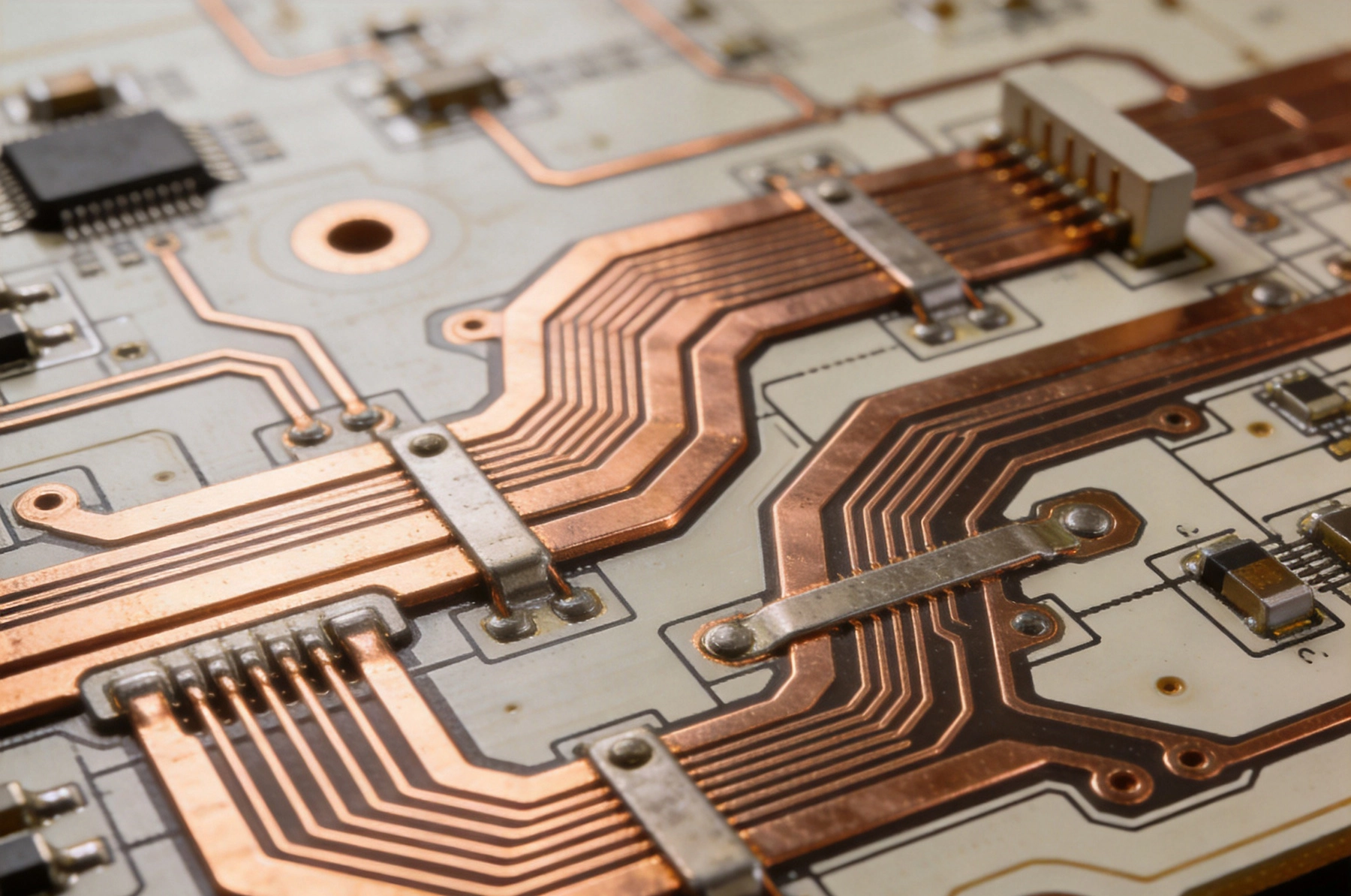
Before comparing routing strategies, we must understand why voltage drop occurs. When current flows through a conductor, the inherent resistance of that conductor converts electrical energy into heat. This voltage reduction follows Ohm's Law: V = I × R. In High Current applications where currents may reach 10A, 20A, or even 100A, even small trace resistances create significant voltage losses.
Trace resistance depends on several factors including conductor width, thickness (Copper Weight), length, and temperature. A trace carrying 20A that experiences 100mV of voltage drop represents 2 watts of power dissipation—energy that doesn't reach your load but instead heats your board.
Voltage drop affects system operation in multiple ways. Downstream components receive less voltage than specified, potentially causing improper operation or reduced performance. Voltage drops across ground traces create offset voltages that interfere with precision analog measurements. Thermal heating from power dissipation accelerates board degradation and may require additional cooling measures.
In battery-powered applications, voltage drop directly reduces available runtime. Every millivolt lost to trace resistance represents energy unavailable for useful work, reducing overall system efficiency and potentially triggering premature low-voltage shutdown.
Daisy-chain routing connects components in a sequential path, where power flows from one component to the next through shared trace segments. Imagine connecting LED modules where each module receives power from the previous one, with a single feed point at the chain's origin. This creates a linear distribution where current passes through intermediate components to reach downstream loads.
The simplicity of daisy-chain routing makes it attractive for many applications. A single wide trace carries current from the power source, branching only at connection points. Routing complexity stays low, and board space requirements remain predictable. This approach works well when component current draw is relatively uniform and physical layout naturally follows a linear arrangement.
The fundamental characteristic of daisy-chain routing is cumulative voltage drop. Components nearest the power source operate at higher voltage than those at the chain's end. If the source provides 12V and each trace segment drops 50mV, the fifth component in the chain receives 12V minus 250mV—significantly lower than the first component.
This voltage gradient becomes more pronounced with longer chains, higher currents, or narrower traces. Designers must calculate voltage at the worst-case location (typically the chain's end) and ensure all components tolerate the minimum expected voltage. Safety margins add complexity and may require larger traces or additional power taps.
Daisy-chain topology performs well when load currents are nearly identical and the cumulative current through shared segments doesn't create excessive voltage drop. LED lighting installations, where strings of identical LEDs receive power, represent a classic application. Motor driver boards where multiple drivers share a common power rail also benefit from sequential routing.
The approach proves particularly valuable when board space is limited or routing flexibility is constrained. A single power spine with distribution branches often requires fewer vias and less routing area than alternative approaches.
Star routing creates dedicated power paths from a central distribution point to each load. Think of a wheel with a hub at the center and spokes radiating to individual components. Each load receives its own trace directly from the power source, eliminating shared current-carrying segments between loads.
This topology requires more routing resources—multiple traces must reach from the central bus to each destination. However, the compensation comes in the form of more uniform voltage distribution. Each load experiences voltage drop only through its own dedicated trace, independent of other loads' current draw.
Voltage drop in star routing depends solely on the trace resistance between the central bus and individual loads. If all traces have similar dimensions, they exhibit similar voltage drops regardless of how many loads are connected. This predictability simplifies design and analysis—you calculate voltage at each load independently rather than tracking cumulative effects through a chain.
The central distribution point experiences High Current concentration as all branch currents combine. This junction requires robust planning—wide traces, thermal relief considerations, and potentially multiple vias in parallel to handle the aggregated current without excessive heating or voltage drop.
Star routing proves essential for sensitive analog circuits where uniform power voltage affects measurement accuracy. Precision sensors, high-resolution data converters, and RF circuits benefit from dedicated power paths that prevent interaction between different circuit sections' current demands.
When loads exhibit variable current draw—such as microprocessors that transition between sleep and active modes—star routing prevents supply voltage fluctuation at one load from affecting others. This isolation simplifies decoupling network design and improves overall circuit stability.
Consider a board with four loads, each drawing 5A, located approximately 50mm from the power source. We'll compare daisy-chain versus star routing for this scenario, assuming trace resistance of approximately 0.5mΩ per millimeter on a standard 3oz Copper Weight configuration.
Daisy-Chain Analysis: If we route power sequentially with 50mm segments between each load, the first load sits 50mm from the source, the second at 100mm, the third at 150mm, and the fourth at 200mm. Current through the shared segment to load four carries 20A (all four loads' current combined), creating substantial drop. The fourth load experiences significantly lower voltage than the first.
Star Routing Analysis: Each load receives its own 50mm trace from the central bus. Each trace carries only its own 5A current. Voltage drop per trace remains uniform across all loads, and while each individual drop may be slightly higher than in daisy-chain (due to zero current-sharing benefit), the distribution is symmetric and predictable.
The crossover point where star routing becomes advantageous depends on trace resistance, current levels, and load distribution. Generally, star routing wins when shared trace segments carry currents approaching or exceeding the sum of downstream loads. Daisy-chain remains competitive when trace segments are short or when intermediate load currents are negligible compared to downstream currents.
For practical board designs, engineers often analyze specific scenarios using Pcb Current calculators or simulation tools. The Ipc-2152 standard provides guidance for current-carrying capacity and temperature rise in Pcb Traces, enabling informed decisions based on actual copper weights and ambient conditions.
Pure daisy-chain or pure star routing rarely represent optimal solutions for complex real-world designs. Most practical high-current PCBs employ hybrid strategies that capture benefits from each approach.
A common hybrid technique divides the board into power zones. A central bus (star characteristics) distributes power to zone entry points, while within each zone (daisy-chain or local star) routes power to individual loads. This approach balances routing efficiency with voltage uniformity.
For instance, an automotive body control module might have dedicated power feeds to front and rear zones from the main battery input. Within each zone, local regulators distribute power to specific control modules through shorter local traces.
Integrating point-of-load (POL) regulators dramatically simplifies power distribution trade-offs. Rather than distributing raw battery voltage throughout the board, POL converters accept wide input voltage ranges and produce tightly regulated outputs exactly where needed. This approach tolerates significant voltage drop in distribution traces because downstream converters compensate.
Modern POL regulators offer efficiencies exceeding 95%, small footprints, and fast transient response. The trade-off includes additional components, complexity, and cost—but for applications where voltage precision matters, the benefits often outweigh these considerations.
Trace current-carrying capacity scales with copper cross-sectional area. Increasing copper weight from 1oz to 2oz doubles the cross-sectional area, approximately halving resistance per unit length. For high current paths, 2oz to 4oz copper weights become necessary, while some Power Electronics use custom Heavy Copper sections exceeding 6oz.
Standard PCB Fabrication offers limited copper weight options, but specialized manufacturers provide heavier copper weights for power-intensive applications. The cost premium often proves worthwhile when voltage drop or thermal issues threaten design success.
Width directly affects resistance—doubling width halves resistance. Using calculators based on Ipc-2152 or internal manufacturer data, designers determine minimum widths for acceptable temperature rise at maximum current. However, minimum-width traces for maximum current rarely represent optimal design; additional width margin improves efficiency and thermal margins.
For very high currents, consider using dedicated Power Planes rather than traces. Planes provide lower resistance than traces of comparable width, distribute current more uniformly, and offer better thermal spreading. However, planes complicate routing for other signals and may conflict with other design requirements.
Vias represent potential bottlenecks in high current paths. A single 0.5mm diameter via might handle 1A safely, but 10A applications require multiple vias in parallel or larger via sizes. Filled vias with thermal relief plating offer current capacity approaching the trace width that the via replaces.
During layout, place vias strategically at current concentration points: power entry, branch points, and component pads. Avoid long strings of vias that each add small resistance—these accumulate to create unexpected voltage drops.
Voltage drop and temperature rise are intimately connected. As current flows through resistance, power dissipates as heat (P = I² × R). This heating raises trace temperature above ambient, potentially affecting nearby components and accelerating board material degradation.
IPC-2152 charts provide temperature rise data for various trace widths, copper weights, and ambient conditions. These charts reveal the non-linear relationship—doubling width doesn't halve temperature rise; instead, the improvement follows diminishing returns. Understanding this relationship helps balance trace width against board space constraints.
Large thermal relief spokes connecting Power Planes to component pads facilitate soldering but increase effective resistance. For high current pads, consider direct connections without thermal relief, accepting the manufacturing challenge in exchange for improved electrical performance.
For components rated for high current, manufacturers often specify pad dimensions and connection patterns that ensure reliable solder joints while minimizing resistance. Following these specifications proves particularly important for current sense resistors, power MOSFETs, and battery connectors.
Convective cooling removes heat from board surfaces. Orienting boards to promote natural airflow across high-current traces improves Heat Dissipation significantly compared to stagnant conditions. Forced airflow from fans or heatsinks may be necessary for extreme current levels, but thoughtful orientation often provides meaningful improvement with minimal cost.
Modern Pcb Design tools increasingly incorporate voltage drop simulation capabilities. These tools model trace geometries, copper weights, and current flows to predict voltage distribution across the board under various load conditions. While accuracy depends on accurate modeling of all current paths, these simulations catch problems before prototype fabrication.
For critical applications, thermal simulation complements electrical analysis. Combined electrical-thermal simulation predicts both voltage drops and resulting temperature rises, identifying hotspots that might cause reliability issues.
Physical measurement validates simulation predictions and reveals issues that modeling might miss. Four-wire Kelvin measurements isolate trace resistance from probe and cable resistances. Thermal imaging identifies hot spots during operation, while voltage probing at various board locations maps actual voltage distribution.
Building prototype boards with test points at strategic locations enables comprehensive validation. These measurements inform production board revisions while there's still opportunity to improve the design.
For identical trace dimensions, star routing typically produces lower maximum voltage drop when loads are distributed at varying distances from the power source. Daisy-chain forces all current for downstream loads through shared segments, increasing drop at the chain's end. Star routing equalizes drop across loads by providing dedicated paths.
Daisy-chain may perform comparably or better when all loads are at similar distances from the source and current levels are uniform. In these cases, the shared trace approaches the total copper of star routing's dedicated traces but with less total metal volume, potentially offering similar drop with lower cost.
Using IPC-2152 guidelines, a 20A trace on an external layer in still air requires approximately 10-12mm width with 1oz copper. Increasing to 2oz copper reduces required width to roughly 5-6mm. Always verify with manufacturer-specific data and consider temperature rise limits for your application.
Sum the I²R losses for each trace segment in the current path. Determine segment currents from load analysis, calculate segment resistances using trace dimensions and copper weight, then multiply to find voltage drop. Simulation tools automate this calculation for complex boards with many interconnected paths.
Power planes offer lower resistance and better heat spreading than traces of comparable width, making them preferred for very high currents. However, planes consume routing space and complicate signal routing. For moderate currents (5-20A), wide traces often suffice; beyond 20A, consider dedicated power planes.
POL regulators accept input voltage variation and produce stable output voltage regardless of distribution losses. This allows narrower traces on the input side since downstream regulators compensate. However, input voltage must remain above the regulator's minimum input specification under worst-case drop conditions.
Voltage drop in High Current PCB design requires careful consideration of routing topology. Daisy-chain routing offers simplicity and routing efficiency but produces non-uniform voltage distribution that may challenge downstream components. Star routing provides uniform power distribution at the cost of increased routing complexity.
Most practical designs benefit from hybrid approaches that combine topology elements strategically. Zone-based distribution, dedicated high-current planes, and point-of-load regulation each address specific challenges while complementing base routing strategies.
Success in High Current Pcb Design ultimately depends on understanding your specific load requirements, tolerance for voltage variation, thermal constraints, and manufacturing considerations. Using quantitative analysis tools alongside practical design guidelines enables decisions that optimize performance within your project's constraints.
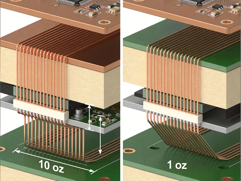
Heavy Copper vs Standard Copper PCB: Complete Comparison Guide for EngineersMay/20/2026
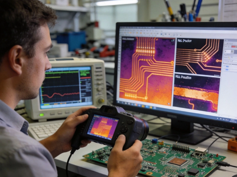
Copper Pour vs Trace: What 3 Years of PCB Failures Taught UsMay/21/2026

Building a High Current PCB Power Supply for Server RacksJuly/30/2026
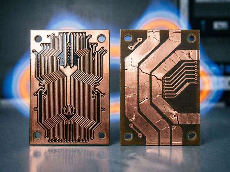
High Current PCB vs. Standard PCB: A Real-World Thermal Stress TestJuly/09/2026
Building a 50A DC-DC Converter: High Current PCB Layout Lessons LearnedJuly/12/2026
High Current PCB Copper Balancing: Preventing Warpage in Heavy Copper BoardsSeptember/07/2026

High Current PCB Design for Railway Traction SystemsAugust/07/2026
High Current PCB Routing: 45-Degree Angles vs. Curved Traces in PracticeJuly/10/2026