

Uninterruptible Power Supplies (UPS) are critical for protecting sensitive electronic equipment from power outages, voltage fluctuations, and surges. From small desktop units protecting home computers to industrial-scale UPS systems protecting data centers, hospitals, and manufacturing facilities, these devices must deliver reliable, clean power continuously, even during extended outages.
At the heart of every UPS is a High Current printed circuit board (PCB) that handles power conversion, battery charging, and Power Distribution. Unlike low-current digital PCBs, High Current UPS PCBs face unique design challenges, including heat management, voltage drop, electromagnetic interference (Emi), and mechanical reliability. Poor High Current Design can lead to reduced efficiency, overheating, component failure, and even catastrophic system failure.
This guide covers the key principles, best practices, and critical considerations for designing reliable, efficient high current PCBs for UPS systems.
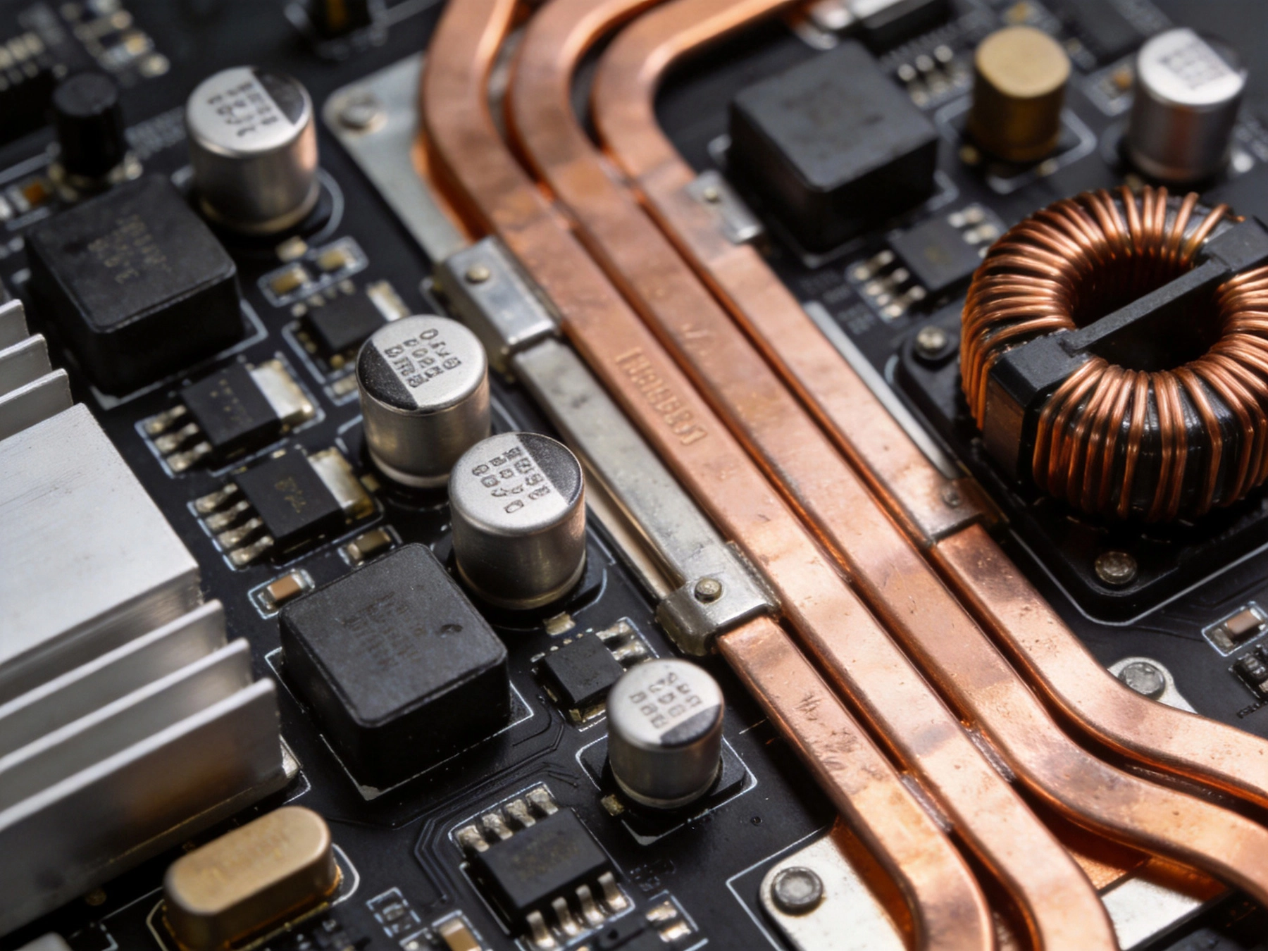
UPS systems handle varying levels of current depending on their power rating and operating mode. Key high current paths in a typical UPS include:
UPS power ratings range from 500VA for small desktop units to 1MVA or more for industrial and data center applications, corresponding to output currents from 2A to thousands of amps at 120V/240V AC. These high current levels require careful Pcb Design to ensure reliable operation.
Unlike consumer electronics that operate intermittently, UPS systems often run 24/7 for 10+ years, making long-term reliability even more critical. High Current Design flaws that would be minor in a consumer product can lead to premature failure in a UPS system operating continuously under load.
Designing high current PCBs for UPS systems presents several unique challenges that must be addressed to ensure reliable operation:
The most significant challenge in High Current PCB design is managing heat generated by I²R losses in copper traces, component leads, and connections. Even small amounts of resistance in high current paths can generate significant heat: a 1mΩ resistance carrying 100A generates 10W of heat. Excessive heat can damage components, degrade PCB materials, and reduce system reliability and lifespan.
High currents flowing through Pcb Traces cause voltage drops that can reduce the efficiency of the UPS and lead to output voltage regulation issues. For example, a 50A current flowing through a trace with 10mΩ resistance causes a 0.5V voltage drop, wasting 25W of power and reducing the output voltage available to the load. In low-voltage, high-current UPS systems, these voltage drops can become significant enough to affect performance.
High currents switching rapidly in inverter and rectifier circuits generate strong electromagnetic fields that can interfere with control circuits, communication systems, and nearby electronic equipment. Large current loops can act as antennas, radiating Emi and causing compliance issues with electromagnetic compatibility (EMC) standards.
High current connections and traces are subject to mechanical stress from Thermal Cycling, vibration, and physical shock. Repeated heating and cooling can cause solder joints to fatigue and fail over time, while high current flowing through poorly made connections can cause localized heating, arcing, and even fire hazards.
UPS systems often contain both high-voltage (line voltage) and low-voltage (battery, control) circuits. Designers must ensure adequate electrical isolation between high-voltage and low-voltage sections to prevent electric shock hazards and damage to low-voltage circuits. High voltage can also arc across improperly spaced traces, leading to short circuits and system failure.
Successful high current UPS Pcb Design requires following several core design principles to address the challenges outlined above:
The most fundamental decision in High Current PCB design is selecting the appropriate Copper Thickness for the board. Standard PCBs use 1oz (35µm) copper, which is insufficient for most high current applications. UPS PCBs typically use:
Copper Thickness directly impacts the Current Carrying Capacity of traces and the Thermal Resistance of the board. Thicker copper allows narrower traces for the same Current Carrying Capacity and improves Heat Dissipation from power components.
The required trace width for a given current depends on the copper thickness, maximum allowable temperature rise, and whether the trace is on an external or internal layer. The Ipc-2221 Standard provides formulas for calculating the minimum trace width for a given current and temperature rise.
For external traces (outer layers) with 10°C maximum temperature rise:
Internal traces have approximately 50% lower current carrying capacity than external traces for the same copper thickness, as they cannot dissipate heat as effectively to the environment.
When calculating trace widths, always include a safety margin of 20-30% to account for manufacturing variations, higher ambient temperatures, and transient current spikes.
For high current UPS PCBs, use dedicated power and ground planes instead of individual traces wherever possible. Planes offer several advantages:
For very high current applications, use multiple copper layers in parallel to carry high currents, effectively increasing the total copper thickness available for power paths.
Vias are often the bottleneck in high current paths, as they have smaller cross-sectional area than traces and can be a source of increased resistance and heat generation. Follow these guidelines for high current vias:
A single 0.8mm via with 25µm plating can carry approximately 5-10A with a 10°C temperature rise, depending on the board thickness and Copper Weight.
Effective Thermal Management is critical for high current UPS PCBs. Key Thermal Design strategies include:
Component layout has a significant impact on the performance and reliability of high current UPS PCBs:
Follow these best practices to optimize your high current UPS PCB design for reliability and performance:
High current loops generate significant EMI and can cause voltage spikes and noise in control circuits. Always place the positive and negative (or phase and neutral) conductors of high current paths as close together as possible, and run them parallel to each other to minimize Loop Area. For plane layers, ensure that return current paths are directly adjacent to the forward current paths to minimize loop area.
Ensure adequate electrical clearance and creepage distance between high-voltage and low-voltage circuits, and between different high-voltage potentials, according to applicable safety standards (such as IEC 60950 for information technology equipment, IEC 62040 for UPS systems, and UL 1778 for uninterruptible power supplies).
For 120V/240V systems, a minimum of 2.5mm clearance and 4mm creepage distance is typically required between primary and secondary circuits, with larger distances for higher voltage systems.
High current connections are common failure points in UPS systems. Follow these guidelines for reliable connections:
UPS systems require accurate current sensing for protection, monitoring, and control. Place current sense resistors or current transformers in high current paths with uniform current flow, away from magnetic fields generated by transformers and inductors. Ensure that the sense traces are routed differentially and away from high current paths to avoid noise interference.
Place high-frequency decoupling capacitors as close as possible to power semiconductor leads to suppress voltage spikes and noise. Use large electrolytic capacitors at the input and output of power stages to smooth current fluctuations and reduce ripple. Place these capacitors as close as possible to the power devices to minimize the length of high current paths.
Include test points for key voltage and current measurements to simplify production testing and troubleshooting. Ensure that high current paths are accessible for current probe measurements during testing. Provide adequate clearances around power components for automated assembly and inspection equipment.
Even experienced designers often make these common high current design mistakes:
After design, thorough testing and validation are critical to ensure the PCB meets performance and reliability requirements:
High Current Pcb Design is a critical factor in the reliability, efficiency, and performance of uninterruptible power supplies. By understanding the unique challenges of high current design, following core design principles, and implementing best practices for layout and thermal management, designers can create UPS PCBs that deliver reliable, efficient operation for 10+ years of continuous service.
Always validate your design through thorough testing and simulation before mass production, and work with an experienced PCB manufacturer that specializes in high current and Heavy Copper Pcb manufacturing to ensure your design is manufactured to the highest quality standards.
A: For a 10kVA UPS with output currents up to 40A at 240V, 4oz (140µm) copper is typically recommended for power layers, with 2oz copper for signal layers. For higher power units with currents over 100A, 6oz or thicker copper may be required.
A: Assuming 0.8mm vias with 25µm plating, each via can carry approximately 10A with a 10°C temperature rise. For 100A, you would need at least 10 vias in parallel, with a safety margin of 20-30% bringing the total to 12-13 vias.
A: Yes, many modern power semiconductors (MOSFETs, IGBTs, diodes) are available in surface-mount packages with high current ratings. However, ensure that the PCB pads are sufficiently large, with adequate copper and Thermal Vias to handle the current and dissipate heat.
A: Use the Ipc-2221 formula or online trace width calculators, which take into account copper thickness, allowable temperature rise, and whether the trace is on an internal or external layer. Always add a 20-30% safety margin to account for manufacturing variations and transient currents.
High Current PCB Pad Design: Reinforced Plating vs. Standard PadsJuly/28/2026
High Current PCB Design for Aerospace Power DistributionSeptember/08/2026
High Current PCB Design for Medical Imaging EquipmentSeptember/10/2026
5 Critical Thermal Management Problems in High Power PCBsMay/21/2026
Designing a High Current PCB for Industrial Welding EquipmentJuly/23/2026
Plated Through Hole Current Rating: Complete Guide for PCB DesignersMay/21/2026
High Current PCB Design GuidelinesMay/21/2026
High Current PCB Current Sensing: Shunt Resistor vs. Hall Effect LayoutJuly/29/2026