

In the rapidly evolving landscape of Power Electronics, the demand forHigh Current PCB Ceramic Substrateshas never been more critical. As we push the boundaries of electric vehicles (EVs), renewable energy systems, and industrial automation, the traditional FR-4 materials simply cannot cope with the thermal and electrical stresses involved. This is where ceramic substrates step in, offering superior thermal conductivity and electrical insulation. However, a common dilemma faced by engineers is choosing between the two dominant technologies: Direct Bonded Copper (DBC) and Active Metal Brazing (AMB). In this article, we will deep dive into the performance comparison of these two technologies to help you make an informed decision for your high-power applications.
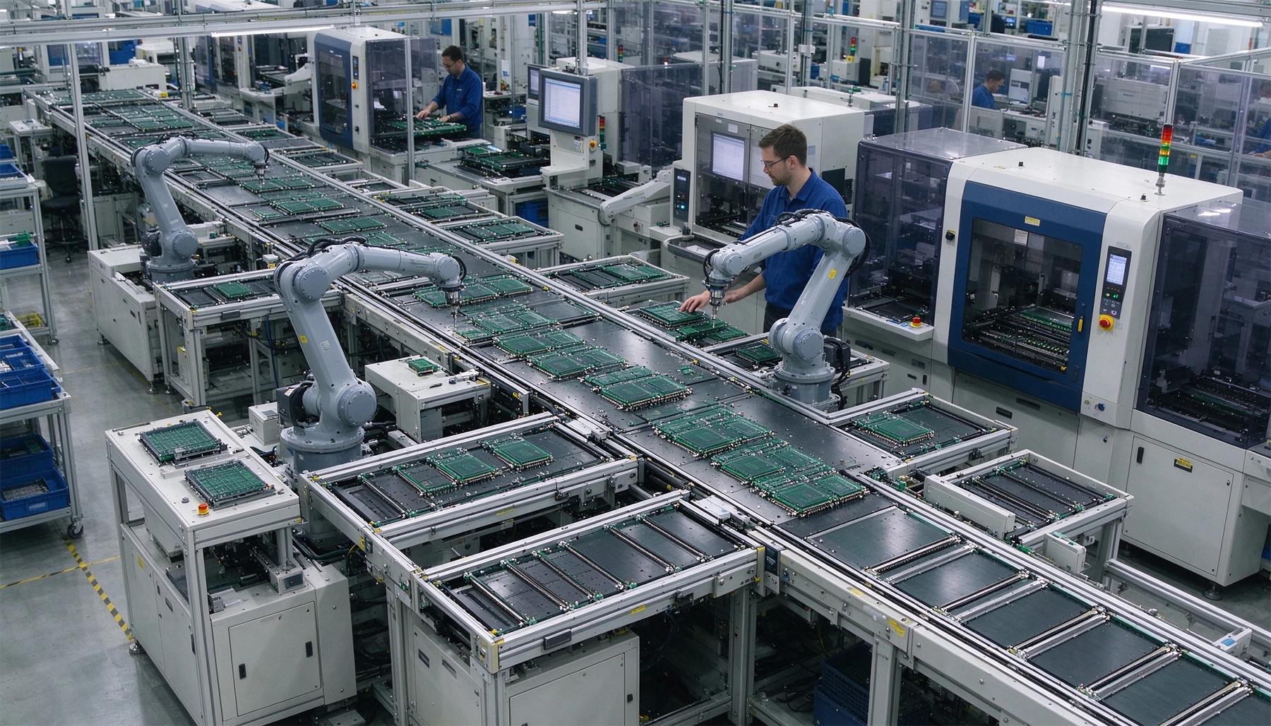
Before we pit DBC against AMB, it is essential to understand what makes a substrate suitable for High Current applications. AHigh Current PCB Ceramic Substratessolution typically utilizes materials like Aluminum Nitride (AlN) or Aluminum Oxide (Al2O3). These ceramics provide a pathway for heat to escape from power modules (like IGBTs or MOSFETs) while electrically isolating the conductive copper layers.
The primary challenge in High Current scenarios is heat generation. If the substrate cannot dissipate this heat efficiently, the component fails. Furthermore, the mechanical bond between the ceramic and the metal must withstand extreme Thermal Cycling without delaminating. This is where the manufacturing process—DBC vs. AMB—becomes the deciding factor.
DBC technology has been the workhorse of the Power Electronics industry for decades. The process involves bonding copper foil directly to the ceramic surface at high temperatures (1065°C - 1083°C) in a nitrogen atmosphere. An oxygen-copper eutectic phase forms at the interface, creating a strong bond.
While DBC is robust, it has limitations. The bond strength, while good, can be susceptible to fatigue under extreme Thermal Cycling conditions. For applications involving Silicon Carbide (SiC) devices which operate at higher junction temperatures, DBC might reach its reliability limits.
AMB is a more advanced joining technology. It uses an active filler metal (usually containing Titanium or Zirconium) that chemically reacts with the ceramic surface to form a bond. This process occurs at lower temperatures than DBC but creates a fundamentally different interface structure.
The primary advantage of AMB lies in its mechanical reliability. The brazing layer acts as a stress buffer, absorbing the mechanical stress caused by the mismatch in the Coefficient of Thermal Expansion (CTE) between the copper and the ceramic. This makes AMB substrates significantly more resistant to thermal cycling.
| Feature | DBC (Direct Bonded Copper) | AMB (Active Metal Brazing) |
|---|---|---|
| Bonding Mechanism | Eutectic bonding (High Temp) | Chemical reaction with active filler |
| Thermal Cycling Reliability | Good | Excellent (Superior for SiC) |
| Peel Strength | High | Very High |
| Cost | Lower | Higher |
| Best Application | Standard IGBT Modules, Consumer Electronics | EV Traction Inverters, Aerospace, High-Power SiC |
When selectingHigh Current PCB Ceramic Substrates, engineers must look beyond just thermal conductivity. Here are the critical factors where DBC and AMB diverge:
In electric vehicles, the power module undergoes constant heating and cooling. AMB substrates have demonstrated the ability to withstand thousands more cycles than DBC before failure. If your design life requires 15+ years of operation in harsh environments, AMB is often the safer choice despite the higher cost.
High current applications require thick copper layers (often 0.6mm to 1.2mm) to minimize resistance. Both DBC and AMB can support thick copper, but AMB's superior bond strength allows it to handle the mechanical stress of these thicker layers better during thermal shocks.
As the industry shifts towards Silicon Carbide (SiC) and Gallium Nitride (GaN), operating temperatures are rising. SiC modules often operate at junction temperatures above 175°C. AMB is widely considered the necessary substrate technology to unlock the full potential of WBG devices.
To illustrate the difference, let's look at two scenarios:
The choice between DBC and AMB for yourHigh Current PCB Ceramic Substratesultimately depends on the specific reliability requirements and budget of your project. DBC remains a fantastic, proven technology for general power electronics. However, as we move towards higher power densities and wide bandgap semiconductors, AMB is becoming the gold standard for reliability.
If you are designing for the next generation of electric mobility or aerospace applications, investing in AMB technology is likely the right move. For cost-sensitive, high-volume commercial products, DBC continues to hold its ground.
The main difference lies in the bonding process. DBC uses a eutectic bond formed at high temperatures, while AMB uses an active metal filler that chemically reacts with the ceramic. This gives AMB better mechanical strength and thermal cycling resistance.
Yes, they can be used, but AMB is generally preferred for high-performance SiC modules due to the higher operating temperatures and the need for superior reliability under thermal stress.
Aluminum Nitride (AlN) is typically the best choice for high current applications due to its high thermal conductivity (approx. 170-180 W/mK) and CTE match with silicon. Aluminum Oxide (Al2O3) is cheaper but has lower thermal conductivity.
Author's Note: With over 10 years of experience in Pcb Manufacturing and supply chain management, I have seen the transition from DBC to AMB firsthand in the EV sector. If you have specific questions about substrate specifications, feel free to reach out.
High Current PCB Surface Finish: ENIG vs. HASL for High Current PadsSeptember/23/2026
High Current PCB Grounding: Star Ground vs. Ground Plane in High Current PathsJuly/31/2026
High Current PCB Current Crowding: Sharp Corners vs. Teardrop TransitionsSeptember/03/2026
Overcoming Voltage Drop in High Current PCB Power Planes: A Case StudyJuly/13/2026
High Current PCB Solder Wicking: Tented Vias vs. Untented ViasSeptember/01/2026
High Current PCB Routing: 45-Degree Angles vs. Curved Traces in PracticeJuly/12/2026
High Current PCB Kelvin Connections: Routing Best Practices for AccuracySeptember/09/2026
High Current PCB Design Guidelines: Ensuring Reliability and SafetyJune/08/2026