

High Current PCB design presents unique challenges that standard surface finish selections may not address. When your board needs to carry tens or hundreds of amperes through power traces and pads, surface finish choice affects Current Carrying Capacity, thermal performance, and long-term reliability of power connections. The standard surface finish comparison between ENIG and HASL takes on different dimensions when current requirements climb beyond typical signal-level applications.
This article examines how surface finish characteristics interact with High Current demands, helping you make informed decisions when specifying finishes for Power Electronics applications. We focus specifically on Heavy Copper designs, power delivery networks, and applications where Current Density becomes a critical design constraint.
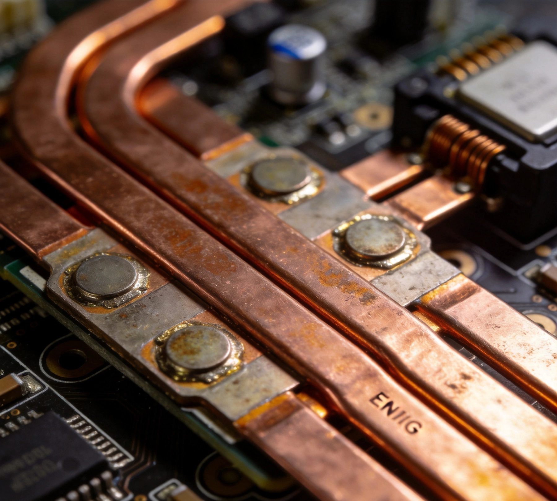
Current flowing through PCB pads and traces encounters resistance that converts electrical energy to heat. This resistance depends on conductor geometry (cross-sectional area and length) and material properties (resistivity of the conductor material). For High Current applications, designers carefully calculate trace width and weight to maintain acceptable temperature rise during operation.
Surface finish adds a layer over the base copper, introducing additional considerations. While this layer is typically thin (measured in microinches), its composition and characteristics affect several factors relevant to high current performance. The interface between the finish layer and underlying copper, the thermal conductivity of the finish material, and the mechanical integrity of the joint between finish and copper all influence how well a pad handles high current flow.
ENIG applies a layer of gold over electroless nickel, with typical thicknesses of 2-5 microinches of gold over 120-240 microinches of nickel. The nickel layer provides structural support and acts as a diffusion barrier preventing copper from migrating into the gold. This structure offers excellent corrosion resistance and maintains solderability over extended periods.
For high current applications, ENIG presents both advantages and concerns. The gold layer has excellent conductivity, though the thin layer thickness means this contributes minimally to overall Current Carrying Capacity. The nickel layer has higher resistivity than copper, and current must pass through this layer at the interface between component leads and the pad surface.
High current operation generates heat, and Thermal Management becomes critical in Power Electronics. ENIG's multilayer structure affects heat transfer between the component and the PCB power plane. The nickel layer has lower thermal conductivity than copper, potentially creating a thermal bottleneck at the pad interface. This Thermal Resistance becomes more significant as current levels increase.
In practical terms, this means ENIG-finished power pads may run slightly hotter than equivalent HASL-finished pads under the same current conditions. For applications operating near thermal limits, this difference can impact component selection or require additional Thermal Management measures such as Thermal Vias, Heat Sinks, or enhanced airflow.
When soldering to ENIG, the solder joint forms with the gold surface, and gold dissolves into the solder during the reflow process. The resulting joint connects primarily to the underlying nickel layer. While this creates reliable joints for signal-level applications, high current flow through these joints raises questions about long-term reliability.
The nickel-solder interface must carry current without degradation over the product lifetime. Under high current stress, this interface may experience electromigration effects or Thermal Cycling fatigue. Engineers designing for extended reliability should consider these mechanisms when specifying ENIG for high current applications.
HASL applies solder directly to the copper surface, typically using tin-lead or lead-free tin-based alloys. The solder layer thickness varies across the pad surface due to the dipping process, but typically ranges from 100-500 microinches depending on board characteristics and processing parameters. This relatively thick solder layer becomes part of the current carrying path.
The solder composition matters for high current performance. Tin-based solders have higher resistivity than copper, though the effect of the thin solder layer is minimal compared to the underlying copper. More importantly, the solder layer distributes current more uniformly across the pad surface than a layered coating, potentially reducing Current Density concentration at specific points.
HASL-finished pads typically show better thermal transfer characteristics than ENIG-finished pads. Since solder is applied directly to copper without an intervening nickel barrier, heat flows more readily from the component lead into the copper plane. This improved thermal conductivity helps manage temperatures in high current applications.
The solder layer also acts as a thermal buffer during current spikes or transient overloads. Solder's lower melting point means it can absorb some thermal energy without the immediate temperature rise that might occur with more rigid metal interfaces. This thermal mass effect provides margin against short-duration overloads.
Solder joints on HASL-finished pads form directly with the base copper, creating a continuous metallic structure from component lead through solder to copper pad. This direct connection provides excellent current transfer characteristics with no intermediate high-resistance layers. The solder joint itself has proven reliability in countless high current applications.
For through-hole components carrying high current, HASL provides another advantage: the solder fills the barrel of the Plated Through-hole during wave or Selective Soldering, creating a substantial current path through the barrel plating. ENIG-finished boards can achieve similar results with appropriate hole preparation, but the process is more straightforward with HASL.
In terms of pure current carrying capacity, both finishes work well when properly applied. The dominant factor in current capacity remains the copper cross-section (trace width times Copper Weight). Surface finish contributes minimally to the overall current path resistance. However, the interface between component lead and pad surface does matter, and HASL typically shows slightly lower contact resistance.
For pad sizes common in high current applications (large enough to handle current flow), the finish contribution to total resistance is typically negligible compared to trace resistance. Design calculations based on copper geometry remain valid regardless of surface finish selection.
Power electronics experience thermal cycles during operation, from ambient temperature changes to self-heating during operation. These thermal cycles stress solder joints as materials expand and contract at different rates. The coefficient of thermal expansion mismatch between component lead material, solder, and PCB substrate creates mechanical stress that can lead to joint degradation over time.
ENIG and HASL joints respond differently to Thermal Cycling. HASL joints form directly with copper, creating a stable interface that tolerates thermal cycling well. ENIG joints involve the gold-solder-nickel structure, which introduces additional material transitions. Some studies suggest HASL joints may have better fatigue resistance in thermal cycling, though both remain acceptable for most applications.
Applications in transportation, industrial equipment, or aerospace face vibration and mechanical shock that stress solder joints. Joint geometry and solder volume affect mechanical robustness. HASL typically provides more solder volume for a given pad size, potentially offering better mechanical robustness under vibration loading.
However, component termination style matters more than surface finish for vibration performance. Proper board design, appropriate component selection, and mechanical mounting provisions typically dominate vibration performance. Surface finish selection should not be the primary driver for vibration-critical applications.
Power supply design typically involves both high current and fine-pitch control circuitry. Many designers specify ENIG for the entire board to simplify manufacturing and ensure compatibility with fine-pitch components while accepting the slight thermal penalty on power pads. This approach works well when power pad current densities are moderate and thermal margins are adequate.
For power supplies with very high current density or tight thermal constraints, selective HASL application makes sense. Apply HASL to power pads and ground planes while using ENIG for signal areas with fine-pitch components. This hybrid approach optimizes both power and signal requirements without compromising either.
Motor drive applications often involve high currents in the power stage alongside control circuits with fine-pitch components for the gate drives and current sensing. HASL works well for the high current motor connection pads and bus bars, while ENIG suits the control circuitry. Many motor drive designs use hybrid approaches to balance these requirements.
For fully through-hole motor drive designs, HASL simplifies assembly by enabling robust Wave Soldering of power components. For surface mount motor drives with BGA or QFN gate drivers, ENIG on signal areas maintains assembly compatibility while HASL handles power pads.
Battery management systems (BMS) must handle high current during charge and discharge while maintaining precise sensing for state-of-charge calculations. The current sensing pads require low-resistance connections for accurate measurements, making HASL a good choice for these nodes. The sense traces themselves often use Kelvin connections with careful layout to ensure measurement accuracy.
For BMS boards with integrated protection circuits using fine-pitch MOSFETs for switching, ENIG on the signal areas ensures reliable assembly of these sensitive components. The high current battery connection pads benefit from HASL's robust joints and excellent thermal transfer.
High power Led Drivers must dissipate significant heat while delivering controlled current to LED arrays. Thermal management is critical for LED lifetime, and the thermal path from LED through PCB to heat sink determines operating temperature. HASL provides better thermal transfer at the LED mounting pads, potentially improving thermal performance.
For Led Drivers with integrated control circuits using microcontrollers or specialized LED driver ICs in fine-pitch packages, ENIG ensures reliable assembly of these sensitive components. The power stage components handling high LED current benefit from HASL finishing on their pads.
Modern Pcb Manufacturing supports selective surface finish application, where different areas of the board receive different treatments. This capability enables optimization of finish selection based on local requirements. High current pads receive HASL or other finishes optimized for power performance, while fine-pitch areas receive ENIG for flatness and solderability.
Selective finish adds some manufacturing complexity and cost, but the benefits often justify this for boards with mixed requirements. When evaluating quotes from manufacturers, ask about their selective finish capabilities and pricing differentials between finish options and combinations.
Very high current applications may require edge plating or separate bus bars in addition to standard surface finish. Edge plating applies thick metal along board edges to create low-resistance current paths for extreme current levels. Bus bars are separate metal components that bolt or solder to the board to handle current flow beyond what traces can accommodate.
For these extreme current applications, surface finish selection on the main board becomes less critical since the current flows primarily through dedicated structures. Standard ENIG or HASL on signal and moderate-power areas works while specialized structures handle extreme current needs.
HASL makes sense for high current applications when thermal transfer is critical, through-hole components handle the primary current flow, vibration or mechanical robustness is a concern, the board uses predominantly through-hole technology without fine-pitch components, or the application requires maximum solder joint volume for mechanical or thermal reasons.
HASL remains the most economical choice for boards without fine-pitch components. When all components have leads suitable for Wave Soldering or hand soldering, HASL provides excellent performance at lower cost than ENIG. The robust solder joints and good thermal transfer support high current operation without compromise.
ENIG is appropriate for high current boards when the assembly includes fine-pitch components requiring flat surfaces, the board design requires multiple reflow cycles, extended shelf life between manufacture and assembly is expected, the application involves wire bonding or other specialized processes, or the manufacturer recommends ENIG for their specific process capabilities.
For mixed-technology boards combining high current power sections with fine-pitch control circuits, ENIG on the entire board is often acceptable. The slight thermal penalty on power pads is typically manageable with proper Thermal Design, and the assembly benefits from consistent finish throughout.
Selective finish application becomes worthwhile when the board has clearly separated high current and fine-pitch areas, Thermal Analysis shows unacceptable temperature rise with uniform ENIG, cost sensitivity allows for selective finishing premium, the manufacturer has proven capability for selective processes, or the performance requirements demand optimization for both power and signal areas.
Evaluate selective finish when designing boards from scratch, as it requires coordination between layout, stack-up planning, and manufacturing process. Retrofitting selective finish to existing designs may require layout modifications to separate finish requirements cleanly.
HASL processing requires careful control of solder temperature, immersion time, and air knife pressure to achieve consistent results. Poorly controlled HASL produces uneven coating thickness that affects coplanarity and may cause problems for surface mount components. Work with manufacturers who demonstrate tight process control for HASL applications.
ENIG processing involves multiple chemical steps including cleaning, microetching, activation, nickel deposition, and gold immersion. Each step requires precise control to achieve consistent coating weight and quality. Black pad defects result from process problems, making manufacturer selection critical for ENIG reliability.
Your assembly process influences finish selection. HASL requires attention to solder temperature profiles since the thick solder layer absorbs more heat during reflow. The component must reach adequate temperature to form good joints without causing damage from excessive heat exposure. Modern lead-free HASL processes operate at higher temperatures than traditional tin-lead, requiring profile adjustment.
ENIG handles reflow profiles well, with the gold surface providing consistent solderability throughout the profile. Components can experience multiple reflow cycles without significant finish degradation, supporting complex assemblies with step soldering or rework operations.
For practical purposes, surface finish does not significantly affect trace current carrying capacity. The trace width and Copper Weight dominate current capacity calculations. Finish thickness is negligible compared to Copper Thickness, and finish resistivity differences do not materially affect total trace resistance. Both ENIG and HASL are acceptable for high current traces when copper sizing is appropriate for the current level.
HASL is generally not recommended for BGA components due to coplanarity variations from the dipping process. BGAs require flat surfaces to ensure all solder balls connect properly during reflow. If your power board includes BGAs for control functions, specify ENIG for those areas while using HASL on power pads. Selective finish enables this optimization.
HASL generally provides better thermal transfer because solder contacts copper directly without an intervening barrier layer. ENIG has the nickel layer that adds Thermal Resistance to the path from component to copper plane. For thermal-critical power applications, HASL on power pads can improve thermal performance by a few degrees compared to ENIG.
Use selective or hybrid finish approaches. Apply ENIG or other flat finishes to areas with fine-pitch components while using HASL on power pads. Many manufacturers offer selective finish processes that apply different treatments to different board areas. Alternatively, specify ENIG on the entire board if thermal margins allow; the slight penalty is often acceptable for the manufacturing simplicity of uniform finish.
Surface finish selection for high current PCBs requires balancing thermal management, mechanical robustness, and manufacturing compatibility. For boards with primarily through-hole components handling high current, HASL provides excellent performance with good thermal transfer and robust joints. For boards combining high current power sections with fine-pitch control circuits, evaluate whether uniform ENIG is acceptable or whether selective finish application better serves the design requirements.
Work with your manufacturer early in the design process to understand their capabilities for different finishes and selective application options. Thermal analysis helps identify whether finish-related thermal differences matter for your specific application. With careful consideration of these factors, you can select the finish approach that best supports your High Current PCB requirements.
High Current PCB Current Crowding: Sharp Corners vs. Teardrop TransitionsSeptember/03/2026
High Current PCB Solder Wicking: Tented Vias vs. Untented ViasSeptember/01/2026
High Current PCB Routing: 45-Degree Angles vs. Curved Traces in PracticeJuly/12/2026
High Current PCB Grounding: Star Ground vs. Ground Plane in High Current PathsJuly/31/2026
Overcoming Voltage Drop in High Current PCB Power Planes: A Case StudyJuly/13/2026
Building a 50A DC-DC Converter: High Current PCB Layout Lessons LearnedJuly/12/2026
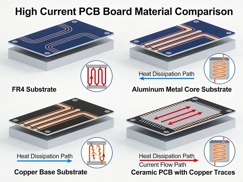
Best Material for High Current PCB Design: How to Choose the Right SubstrateJune/05/2026
High Current PCB Current Sensing: Shunt Resistor vs. Hall Effect LayoutJuly/29/2026