

High-power LED applications demand robust Pcb Design strategies that can handle substantial current loads while maintaining thermal efficiency and electrical reliability. As LED technology continues to advance, drivers must deliver increasingly higher currents to achieve greater light output, pushing conventional Pcb Design approaches to their limits. Understanding the principles of High Current PCB design becomes essential for engineers developing reliable, efficient LED driver systems that can operate safely under demanding conditions.
The challenge in designing PCBs for high-power LED drivers lies in balancing multiple competing requirements: sufficient current-carrying capacity, effective Heat Dissipation, compact form factors, and cost-effectiveness. Unlike low-Power Electronics where trace width and Copper Thickness are secondary considerations, these parameters become critical design factors that directly impact performance, reliability, and longevity. A poorly designed High-current Pcb can lead to excessive voltage drops, thermal runaway, component failure, and potential safety hazards.
This comprehensive guide explores the fundamental principles and best practices for High Current PCB design specifically tailored to high-power LED driver applications. From Copper Thickness selection and Thermal Management strategies to layout optimization and material considerations, we'll cover everything you need to know to create PCBs that can reliably handle the demanding requirements of modern LED lighting systems.
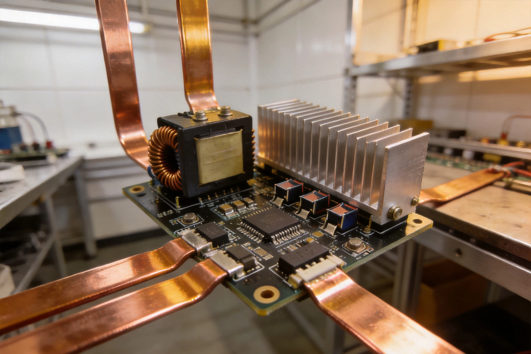
The first step in designing a High-current Pcb for LED drivers is accurately understanding and calculating the current requirements of your application. LED drivers typically need to supply currents ranging from hundreds of milliamps for low-power applications to several amps for high-power LED arrays and modules. The current requirements depend on factors such as the number of LEDs in series or parallel, the forward voltage of each LED, and the desired light output level.
For series-connected LED strings, the current through each LED is the same, making current calculation relatively straightforward. However, the total current requirement increases with the number of parallel strings. For example, a driver powering three parallel strings of high-power LEDs, each drawing 700mA, must deliver a total of 2.1A. This current must flow through the Pcb Traces connecting the driver output to the LED array, making trace design critical for maintaining efficiency and preventing excessive voltage drop.
It's important to consider not just the steady-state current but also peak currents and transient conditions that may occur during startup, dimming transitions, or fault conditions. LED drivers often incorporate soft-start features that gradually increase current, but fault conditions such as short circuits can cause sudden current spikes that exceed normal operating levels. Your PCB design must accommodate these worst-case scenarios without sustaining damage or creating safety hazards.
Analyzing how current distributes through your Pcb Layout helps identify potential bottlenecks and hotspots before fabrication. In LED driver circuits, current typically flows from the power input through switching components, inductors, and output stages to the LED array. Each stage of this path may carry different current levels, requiring different trace widths and copper thicknesses. The highest current paths, typically the output stage connecting to the LEDs, demand the most attention in terms of current-carrying capacity.
Current sharing between parallel LED strings presents another design consideration. Ideally, each string should receive equal current, but slight variations in LED forward voltage or trace resistance can cause imbalances. Proper Pcb Layout can help minimize these imbalances by ensuring symmetrical current paths and equal trace resistances to each string. This becomes particularly important in high-current applications where small resistance differences can lead to significant current variations.
Return current paths are equally important and often overlooked. The current flowing to the LEDs must return to the driver through ground paths, and these return paths should be designed with the same care as the forward current paths. High-current return currents flowing through narrow ground traces can create voltage drops that affect circuit performance and create electromagnetic interference (EMI) issues. Proper ground plane design is essential for handling high return currents effectively.
Copper thickness is perhaps the most critical parameter in high-current PCB design, directly determining the current-carrying capacity and thermal performance of traces. Standard PCB copper thickness is measured in ounces per square foot, with 1oz copper representing approximately 35 microns of thickness. For high-current LED driver applications, thicker copper is typically required to handle the substantial current flows without excessive voltage drop or temperature rise.
The relationship between copper thickness, trace width, and current capacity follows well-established engineering principles, though practical design requires consideration of multiple factors beyond simple ampacity charts. Thicker copper provides lower resistance, reducing voltage drop and power dissipation in traces. This is particularly important in LED driver applications where voltage drops directly affect LED brightness and efficiency. A 2oz Copper Trace has approximately half the resistance of a 1oz trace of the same width, significantly reducing voltage drop and power loss.
However, thicker copper comes with tradeoffs including increased cost, longer etching times, and potential challenges with fine-pitch features. Most PCB manufacturers offer copper thicknesses ranging from 0.5oz to 6oz or more, with 2oz being a common choice for high-current applications. For LED drivers handling currents above 5A, 3oz or 4oz copper may be justified despite the higher cost, particularly when efficiency and thermal performance are critical requirements.
Determining the appropriate trace width for high-current LED driver circuits requires considering both current capacity and acceptable voltage drop. The Ipc-2152 standard provides guidelines for current-carrying capacity based on Copper Weight, trace width, and temperature rise. However, these guidelines represent conservative estimates, and actual requirements may vary based on your specific application constraints and Thermal Management approach.
For LED driver applications, voltage drop often becomes the limiting factor rather than current capacity. Even if a trace can theoretically handle a certain current without exceeding temperature limits, the voltage drop across that trace may be unacceptable for maintaining proper LED operation. A common design target is to limit voltage drop to less than 2% of the supply voltage, though this may vary based on specific application requirements. This voltage drop constraint often drives trace width selection more than pure current-carrying capacity.
Temperature rise calculations must consider the ambient operating environment and the PCB's thermal management capabilities. LED drivers often operate in enclosed fixtures with limited airflow, making thermal management particularly challenging. In these environments, traces may reach higher temperatures than in open-air conditions, potentially requiring wider traces or thicker copper than standard calculations suggest. Conservative design margins help ensure reliable operation across all expected operating conditions.
Thermal management represents one of the most critical aspects of high-power LED driver PCB design. LED drivers generate significant heat from power losses in switching components, inductors, and the Pcb Traces themselves. This heat must be effectively dissipated to prevent component degradation, maintain efficiency, and ensure reliable operation. Poor thermal management can lead to reduced component lifespan, thermal runaway, and potential safety hazards.
The Thermal Design of an LED driver PCB must consider multiple heat sources and their interactions. Switching MOSFETs and diodes generate heat from switching losses and conduction losses. Inductors produce heat from winding resistance and core losses. Even the PCB traces themselves generate heat from I²R losses, particularly when carrying high currents. All these heat sources must be managed collectively to maintain acceptable component and board temperatures.
Thermal management strategies typically combine multiple approaches including proper Component Placement, Copper Pour areas, Thermal Vias, and external heatsinking. The goal is to create efficient thermal paths that conduct heat away from heat-generating components to areas where it can be dissipated, whether through the PCB itself, attached heatsinks, or the surrounding environment. A well-designed thermal management approach can significantly improve reliability and efficiency while allowing for more compact designs.
Copper Pour areas represent one of the most effective thermal management techniques in LED driver PCB design. These large copper areas act as heat spreaders, distributing heat from hotspots across a larger surface area for more efficient dissipation. For high-current LED drivers, copper pours should be strategically placed around high-power components such as MOSFETs, diodes, and inductors to provide thermal relief and improve heat distribution.
Ground planes serve dual purposes in LED driver circuits, providing both electrical grounding and thermal management. A continuous ground plane on one or more layers offers excellent thermal conductivity, helping to distribute heat across the entire board. This is particularly effective for multilayer PCBs where Thermal Vias can connect surface-mount components to internal ground planes, creating efficient thermal paths through the board thickness.
The size and placement of copper pour areas should be optimized based on Thermal Analysis and space constraints. While larger copper areas provide better thermal performance, they may consume valuable board space needed for routing and components. Thermal simulation tools can help identify optimal pour sizes and placements, ensuring effective thermal management without unnecessarily increasing board size or complexity. In many cases, strategically placed copper pours around the hottest components provide the best balance of thermal performance and space utilization.
Proper Component Placement and layout are fundamental to successful high-current LED driver PCB design. The physical arrangement of components affects current paths, thermal management, EMI performance, and overall reliability. A well-planned layout minimizes current loop areas, reduces parasitic inductance and resistance, and facilitates efficient Heat Dissipation, all of which contribute to better performance and reliability.
High-current components should be placed to minimize the length of current-carrying traces. Shorter traces reduce resistance, voltage drop, and power loss, while also minimizing parasitic inductance that can affect switching performance. The switching MOSFET, output inductor, and output capacitor should form a compact loop to minimize high-frequency current paths that can generate EMI. This compact loop also reduces trace inductance, improving switching efficiency and reducing voltage spikes.
Thermal considerations should drive component placement decisions. Heat-generating components such as MOSFETs, diodes, and inductors should be distributed across the board rather than clustered together, preventing local hotspots. When clustering is necessary due to circuit requirements, additional thermal management measures such as copper pours, thermal vias, or external heatsinks become even more critical. Components should also be positioned to facilitate efficient airflow or heat transfer to any attached heatsinks.
Routing high-current paths requires careful attention to trace width, layer selection, and overall path geometry. The highest current paths, typically from the driver output through inductors and switching components to the LED array, should use the widest practical traces and preferably multiple layers in parallel. Multilayer PCBs offer the advantage of being able to route high-current traces on multiple layers connected by numerous vias, effectively increasing the cross-sectional area and reducing resistance.
Via selection and placement become critical in high-current designs. Standard vias may not provide sufficient current-carrying capacity for very high currents, requiring multiple vias in parallel or larger via sizes. Thermal vias should be placed under high-power components to provide thermal paths to internal copper planes or backside copper areas. These vias should be numerous and strategically positioned to create efficient thermal conduction paths without compromising mechanical integrity or manufacturability.
Minimizing current loop area is particularly important for the high-frequency switching currents present in LED drivers. Large current loops act as antennas, generating EMI that can interfere with other circuits or fail electromagnetic compatibility (EMC) requirements. The critical high-frequency loop formed by the switching MOSFET, output inductor, and input/output capacitors should be kept as small as possible, ideally with components placed adjacent to each other and connected with short, direct traces.
The choice of PCB substrate material significantly impacts the performance and reliability of high-current LED driver designs. While standard FR-4 material works adequately for many applications, high-power LED drivers often benefit from specialized materials with better thermal and electrical properties. Understanding the material options and their characteristics helps in selecting the most appropriate substrate for your specific application requirements.
Thermal conductivity represents one of the most important material characteristics for LED driver applications. Standard FR-4 has relatively low thermal conductivity (approximately 0.3-0.4 W/m·K), which limits its ability to conduct heat away from hot components. High-thermal-conductivity materials such as metal-core PCBs (MCPCBs) or ceramic substrates can provide significantly better thermal performance, though at higher cost. For extremely high-power applications, metal-core PCBs with aluminum or copper bases offer excellent thermal conductivity and can effectively replace or supplement traditional heatsinking.
Dielectric constant and loss tangent become important considerations for high-frequency switching circuits. LED drivers operating at high switching frequencies benefit from materials with lower dielectric constants and loss tangents, which reduce parasitic capacitance and dielectric losses. Some high-performance FR-4 materials offer improved high-frequency characteristics compared to standard grades, making them suitable for high-frequency LED driver applications without the cost of more exotic materials.
Metal core PCBs (MCPCBs) represent an excellent solution for high-power LED driver applications where thermal management is critical. These boards use a metal base (typically aluminum or copper) as both the structural substrate and thermal conductor, with a thin dielectric layer separating the metal base from the copper circuit layer. The metal base provides excellent thermal conductivity, effectively spreading heat from components across a large surface area for efficient dissipation.
Aluminum MCPCBs offer a good balance of thermal performance, weight, and cost, making them popular for LED lighting applications. Copper MCPCBs provide even better thermal conductivity but at significantly higher cost and weight. The choice between aluminum and copper depends on your specific thermal requirements and budget constraints. Both types provide substantially better thermal performance than standard FR-4, often eliminating the need for additional heatsinking in moderate-power applications.
The dielectric layer in MCPCBs represents a critical design consideration. This layer must provide adequate electrical insulation while maintaining good thermal conductivity. Thinner dielectric layers provide better thermal performance but may have higher breakdown voltage limitations. Selecting the appropriate dielectric thickness and material requires balancing electrical isolation requirements with thermal performance needs. Many MCPCB manufacturers offer various dielectric options optimized for different voltage and thermal requirements.
Establishing and following comprehensive design rules helps ensure consistent, reliable high-current LED driver PCB designs. These rules should address all aspects of the design including trace widths, spacing, via requirements, thermal management, and manufacturability. Well-defined design rules help avoid common pitfalls and ensure that designs meet both electrical performance and manufacturing requirements.
Trace width rules should be established based on current requirements, acceptable voltage drop, and thermal constraints. Create a trace width table that specifies minimum widths for different current levels, considering both internal and external layers. These rules should account for the specific copper thickness used in your design and include appropriate safety margins. Remember that internal layers typically have different current-carrying capabilities than external layers due to different thermal environments.
Spacing rules become particularly important in high-voltage LED driver applications. Maintain adequate clearance between high-voltage traces and low-voltage circuitry to prevent arcing and ensure safety. Spacing requirements depend on the voltage levels involved and should follow relevant safety standards such as UL or IEC requirements. Even for lower-voltage applications, maintaining adequate spacing helps prevent manufacturing defects and improves reliability.
Comprehensive testing and validation are essential for confirming that your high-current LED driver PCB design meets performance and reliability requirements. Testing should begin with electrical verification of current-carrying capacity, voltage drop, and thermal performance under expected operating conditions. This testing helps identify any design issues before mass production, preventing costly recalls or field failures.
Thermal testing should measure component and board temperatures under various operating conditions, including maximum load and elevated ambient temperatures. Infrared thermography provides valuable insights into thermal distribution and can identify unexpected hotspots that may require design modifications. Thermal testing should also verify that any attached heatsinks or thermal management features perform as expected.
Current capacity testing should verify that all traces and vias can handle their specified currents without excessive temperature rise or voltage drop. This testing should include both steady-state conditions and transient conditions that may occur during startup or fault scenarios. Accelerated life testing under elevated temperature and current conditions can help validate long-term reliability and identify potential failure modes before they occur in the field.
Underestimating current requirements represents one of the most common and costly mistakes in high-current LED driver PCB design. Designing for nominal current levels without considering peak currents, fault conditions, or future expansion can lead to trace overheating, voltage drops, and premature failures. Always design with appropriate safety margins and consider worst-case operating scenarios rather than just typical conditions.
Neglecting thermal management is another frequent error that can have serious consequences. Many designers focus on electrical performance while overlooking thermal considerations, assuming that components will remain within their operating temperature ranges. However, high-power LED drivers generate substantial heat that must be actively managed. Failing to provide adequate thermal paths, copper areas, or heatsinking can lead to component degradation, reduced efficiency, and potential safety hazards.
Improper via usage in high-current paths represents another common mistake. Using standard vias for high-current applications can create bottlenecks and hotspots due to limited current-carrying capacity. High-current paths should use multiple vias in parallel or larger via sizes to ensure adequate current capacity. Additionally, thermal vias under high-power components should be numerous and properly sized to provide effective thermal conduction to inner layers or backside copper.
Q: What copper thickness should I use for a 5A LED driver?
A: For a 5A LED driver, 2oz copper (70μm) represents a good starting point, though 3oz may be justified if efficiency is critical or space is limited. The exact choice depends on your specific requirements for voltage drop, temperature rise, and board space. Calculate trace widths based on your acceptable voltage drop and temperature rise, then verify that the chosen copper thickness can accommodate these widths within your space constraints.
Q: How do I determine the appropriate trace width for high-current paths?
A: Trace width determination should consider both current capacity and voltage drop. Start with Ipc-2152 guidelines for current capacity based on your copper thickness and acceptable temperature rise. Then calculate the voltage drop for this trace width at your maximum current. If the voltage drop exceeds your acceptable limit (typically 2% of supply voltage), increase the trace width accordingly. Remember to include safety margins and consider worst-case operating conditions.
Q: Should I use a Metal Core Pcb for my LED driver?
A: Metal core PCBs offer excellent thermal performance and are particularly beneficial for high-power LED drivers (typically above 50W) where thermal management is challenging. For lower-power applications or designs with good thermal management through other means, standard FR-4 may be adequate and more cost-effective. Consider the total power dissipation, operating environment, and thermal management requirements when deciding whether MCPCBs are justified for your application.
Q: How many thermal vias do I need under a high-power MOSFET?
A>The number of thermal vias depends on the power dissipation and desired thermal performance. A common approach is to use a grid of thermal vias under the MOSFET pad, with via spacing of 1-2mm. For very high-power dissipation (above 5W), use as many vias as practical within the component footprint area. The vias should connect to large copper areas or internal planes to provide effective thermal paths. Thermal simulation can help determine the optimal via quantity and placement.
Q: Can I use the same trace width for all high-current paths?
A>Not necessarily. Different sections of high-current paths may carry different current levels or have different voltage drop requirements. For example, traces connecting to parallel LED strings may carry different currents depending on the number of strings. Analyze the current in each section of your high-current paths and size traces accordingly. Using appropriately sized traces for each current level optimizes space utilization while ensuring adequate performance.
Designing high-current PCBs for high-power LED drivers requires careful consideration of multiple interrelated factors including current capacity, thermal management, component placement, and material selection. Success in this domain comes from understanding how these factors interact and optimizing the design to balance competing requirements. A well-designed high-current PCB not only meets electrical performance specifications but also ensures reliable operation under demanding conditions.
The principles and best practices outlined in this guide provide a foundation for developing effective high-current LED driver PCBs. However, each application presents unique challenges that may require customized solutions. Thermal simulation, prototyping, and comprehensive testing remain essential steps in the development process, helping to validate design decisions and identify areas for improvement before mass production.
As LED technology continues to advance and power levels increase, the importance of proper high-current PCB design will only grow. By mastering these design principles and staying current with emerging technologies and materials, engineers can develop LED driver systems that deliver higher performance, greater reliability, and improved efficiency. The investment in proper PCB design pays dividends throughout the product lifecycle, from initial development through long-term field operation.
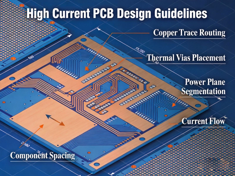
High Current PCB Design GuidelinesMay/21/2026
High Current PCB Design for Telecommunications Base StationsSeptember/18/2026
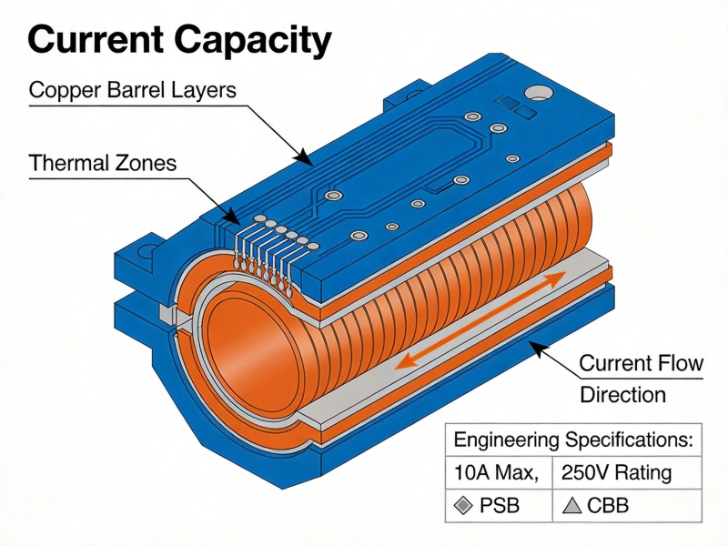
Plated Through Hole Current Rating: Complete Guide for PCB DesignersMay/21/2026
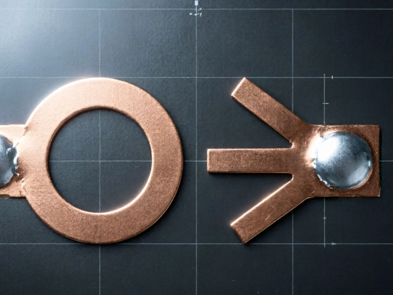
High Current PCB Thermal Relief: Full Connect vs. Modified SpokesJuly/16/2026
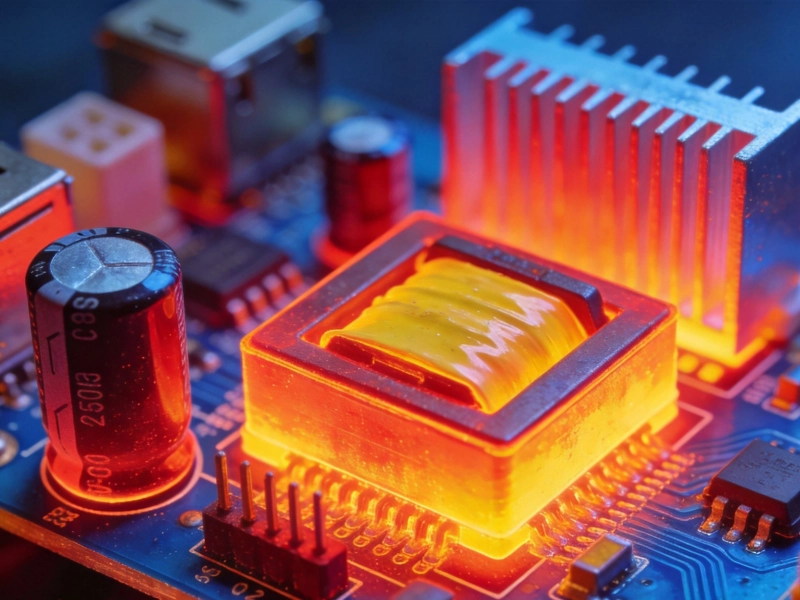
High Current PCB Design for High-Frequency Switching RegulatorsSeptember/04/2026
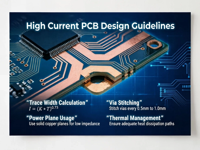
High Current PCB Design Guidelines: Ensuring Reliability and SafetyJune/08/2026
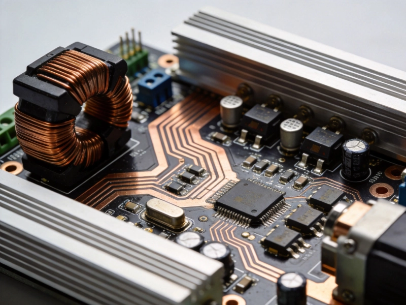
High Current PCB Design for Robotics Motor ControllersSeptember/16/2026
Designing a High Current PCB Motor Driver: Avoiding EMI PitfallsJuly/14/2026