

High-frequency switching regulators power everything from server motherboards to Automotive Electronics. At frequencies above 500 kHz—and increasingly pushing past 1 MHz—these power conversion circuits demand PCB layouts that would make an aerospace engineer nervous. The difference between a reliable power supply and a smoking crater often comes down to a few mils of trace width or a poorly placed Decoupling Capacitor.
This guide covers the essential Pcb Design considerations for high-current, high-frequency switching regulators. Whether you're working with synchronous buck converters, boost converters, or LLC resonant topologies, these principles will help you avoid the most common layout pitfalls.
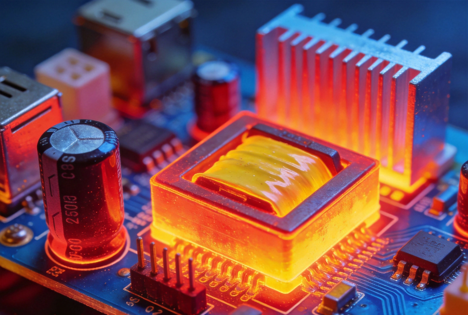
Before diving into layout specifics, it's worth understanding why frequency matters so much in switching regulator design.
At low switching frequencies, PCB parasitics barely register. A few nanohenries of trace inductance? Irrelevant when your edges are microseconds wide. But push into the megahertz range, and those same parasitics become the dominant circuit elements. Your carefully designed compensation network becomes a noise generator. Your input filter oscillates with your gate drive. Your output voltage rings like a bell every time the high-side MOSFET turns on.
Higher frequencies also mean smaller inductors and capacitors—which is great for size reduction—but they make the Pcb Layout exponentially more critical. Every picosecond of skew between switching nodes matters. Every square of copper resistance adds up. Every thermal hotspot becomes a reliability concern.
If you remember nothing else from this article, remember this: the switching current loop must be as small and tight as possible. This loop consists of the path current takes during the brief transition when the MOSFET switches states.
In a synchronous buck converter, two distinct current loops exist:
Both loops need to be minimized, but the input loop is typically more critical because it connects directly to the noisy switching node.
Place input bypass capacitors directly adjacent to the MOSFETs—ideally on the same layer, directly beneath or beside the switching devices. The goal is to create a Loop Area measured in square millimeters, not square centimeters.
Use ground planes strategically to contain magnetic field radiation. A solid ground plane beneath the current loop acts as a shield, containing the fields and reducing both radiated Emi and coupled noise to sensitive circuits.
Avoid routing high-current paths through vias. Vias add inductance and resistance. When you must use vias for thermal relief or layer changes, use multiple smaller vias in parallel rather than one large via—and ensure the via barrel is properly plated.
The switching node is where voltage swings between input and ground at speeds measured in nanoseconds. This node is simultaneously your greatest noise source and your most layout-sensitive net.
The switching node should be as compact as possible. A large switching node acts like an antenna, radiating EMI everywhere. Keep the node small, and keep it away from sensitive traces—especially feedback paths, compensation components, and analog ground returns.
In practice, this often means placing the MOSFETs, inductor, and input caps in a tight cluster with short, wide traces connecting them. Yes, the inductor connection to the output will be a high-current trace—but it doesn't switch at high di/dt, so it's less critical for EMI.
Keep the switching node away from feedback dividers, soft-start circuits, and other sensitive nodes. Even a few hundred mils of proximity can couple enough noise to cause instability or excessive output ripple.
If your layout requires routing near the switching node, use ground traces or planes as guard bands between the noisy net and sensitive circuits.
High-current switching regulators dissipate significant power in the MOSFETs, inductor, and Pcb Traces themselves. Effective Thermal Management isn't optional—it's a reliability requirement.
For high-current traces, Ipc-2152 provides the standard reference for current-carrying capacity. But IPC's charts assume ambient conditions that may not match your application. A trace in a sealed enclosure with poor airflow will run much hotter than IPC predicts.
For internal layers (buried in the PCB stackup), current capacity drops significantly—typically by 50% or more compared to surface traces. If your high-current path must use internal layers, increase trace width accordingly or add Thermal Vias to transfer heat to external planes.
For typical 2 oz copper on outer layers, expect approximately 20-25 A per millimeter of trace width for a 10°C temperature rise. But always validate with thermal simulation or measurement, especially for critical applications.
Rather than traces, consider using copper planes for high-Current Distribution. Planes provide lower resistance, better heat spreading, and more predictable thermal behavior. The key is ensuring the plane is continuous and uninterrupted by slots or anti-pads that force current to take a longer path.
For buck regulators, the input and output planes should be on adjacent layers to create effective decoupling while minimizing Loop Area. Place the ground plane between them for isolation and noise control.
Thermal Vias transfer heat from internal layers to external heatsinking surfaces. Use a matrix of small vias (typically 0.3-0.5 mm diameter) rather than fewer large vias—the smaller vias provide better thermal transfer with less inductance.
For packages like QFN or BGA where thermal performance depends on the PCB, ensure thermal vias are placed directly under the Thermal Pad and are properly plated to minimize Thermal Resistance. Void-free plating is critical; voids act as thermal insulators.
Grounding in switching regulators is often misunderstood. The goal isn't to create a single, quiet ground—it's to manage return currents and prevent noise coupling.
Separate signal ground from power ground at a single point, typically near the output capacitor return. This prevents high-current switching currents from flowing through sensitive analog ground returns.
The feedback voltage divider, compensation components, and any analog circuits should connect to a quiet ground reference—ideally the output capacitor return, which sees minimal AC switching current.
For output voltage sensing, use a Kelvin Connection to the load. This means running a separate, dedicated trace from the actual load point back to the feedback divider, rather than relying on the high-Current Return Path. The voltage drop in the high-current trace would otherwise cause significant regulation error.
For boards with multiple power rails, consider a star ground pattern where all grounds connect at a central point. This prevents one rail's switching noise from propagating into another's ground reference. The star point should be at the main input capacitor ground, where all power currents ultimately return.
High-frequency switching regulators are prolific EMI generators. Passing CISPR or FCC compliance testing requires attention to both conducted and radiated emissions.
Place input EMI filters as close to the regulator as possible. The filter should include both differential-mode and common-mode components. For differential mode, use X7R or X5R ceramic capacitors sized according to your switching frequency and expected ripple current.
Common-mode filtering requires common-mode chokes, which can be either discrete components or integrated into the input wiring. Don't neglect the common-mode path—it's often the dominant mechanism for radiated emissions.
Switching nodes often exhibit voltage overshoot and ringing due to Parasitic Inductance resonating with MOSFET capacitance. A properly sized RC snubber absorbs this energy, reducing both EMI and stress on the MOSFET.
Place the snubber directly across the switching node—ideally on the same layer, as close as possible to the MOSFET. The resistor should be rated for the transient power, and the capacitor should be a high-voltage, low-inductance type (film or C0G ceramic).
For applications requiring strict EMI performance, consider using a metal enclosure or shield cans over the switching regulator. The shield should be connected to ground with multiple low-inductance points to be effective.
Be aware that shields can create cavities that resonate at frequencies determined by the cavity dimensions. If your switching frequency or harmonics fall within a resonant mode, you may need absorptive materials inside the cavity.
The physical placement of components determines your layout success before you draw a single trace. Here's how to think about placement for switching regulators.
Place these components first, as they constrain everything else:
Place sensitive components in areas isolated from switching noise:
For controllers driving external MOSFETs, gate drive traces are critical. These traces should be short, direct, and paired (gate and return) to minimize loop area. Avoid running gate drive traces near noisy switching nodes or sensitive analog circuits.
If using gate drive transformers or optocouplers, place them close to both the controller and the MOSFET to minimize the high-frequency pulse path.
Your PCB stackup significantly impacts switching regulator performance. Here are recommendations for common scenarios.
For cost-sensitive applications, a 4-Layer Stackup can work well:
Keep the gap between Layer 1 and Layer 2 small (2-4 mils) to minimize loop areas for signals on the top layer.
For complex multi-rail systems or very High Current, additional layers provide flexibility:
The key principle is maintaining continuous ground planes adjacent to high-speed signal layers to provide controlled impedance and shielding.
Modern EDA tools include powerful simulation capabilities that can catch layout issues before you build hardware.
Power delivery network (Pdn) analysis tools simulate the impedance between the regulator output and the load. A high impedance at the switching frequency can cause instability or excessive ripple.
Several tools can predict radiated emissions from PCB layouts, giving you a chance to correct problems before sending files to fabrication. While not as accurate as chamber testing, these tools identify obvious issues and help prioritize design changes.
Thermal simulation tools model heat transfer from components through the PCB to ambient air. These simulations are particularly valuable for high-current designs where thermal margins may be tight.
After working with dozens of high-frequency switching regulator designs, certain mistakes appear repeatedly. Here's what to watch for:
Designing PCBs for high-frequency switching regulators is a discipline that rewards attention to detail. The layout determines whether your regulator performs at its theoretical efficiency or burns up in a blaze of EMI and thermal failure.
Focus on the fundamentals: minimize current loop areas, manage thermal performance, separate sensitive circuits from noise sources, and validate your design through simulation and testing. These principles don't change regardless of switching frequency or topology.
As frequencies continue climbing and power densities increase, the importance of good layout practice only grows. Invest the time upfront to get the layout right—it costs far less than debugging a failing design or re-spinning boards.
For 10A continuous current on 2 oz copper outer layer, minimum trace width is typically 0.5-1mm. However, always verify with Thermal Analysis for your specific conditions. Internal layer traces require significantly more width due to reduced cooling.
Optimize the layout first—minimize loop areas and switching node size. Proper placement and ground plane strategy can reduce emissions by 20 dB or more before adding any filtering components.
Oscillation despite correct compensation usually indicates layout problems. Check for long gate drive traces, inadequate input decoupling, or noise coupling into the feedback path. A Kelvin Connection at the output can also help if there's significant voltage drop in the return path.
Place capacitors directly adjacent to the MOSFETs on the same layer. Use wide, short traces or direct pad connections. Avoid routing through vias to the capacitors—the via inductance appears directly in your critical switching loop.
A minimum of 4 layers is recommended for frequencies above 500 kHz. This allows dedicated ground planes and power planes that minimize loop areas and provide shielding. Complex designs may benefit from 6 or more layers for better Signal Integrity and Thermal Management.
Need help optimizing your switching regulator Pcb Layout? Our engineering team specializes in high-power, high-frequency designs for demanding applications.
A Deep Dive into High Current PCB Design for Solar InvertersJuly/17/2026
High Current PCB Design for Renewable Energy MicrogridsSeptember/30/2026
High Current PCB Design for Electric Forklifts: A Practical Engineering GuideOctober/13/2026

High Current PCB Design for Data Center Power ShelvesOctober/19/2026
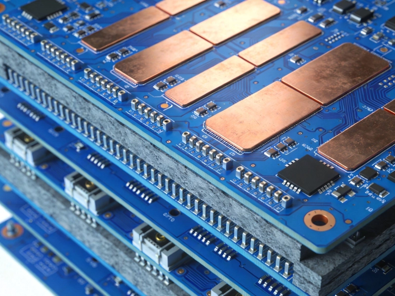
High Current PCB Design for Telecommunications Base StationsSeptember/18/2026
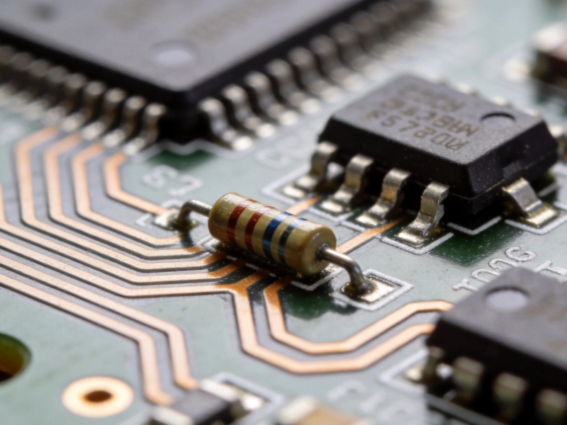
High Current PCB Current Sensing: Shunt Resistor vs. Hall Effect LayoutJuly/29/2026
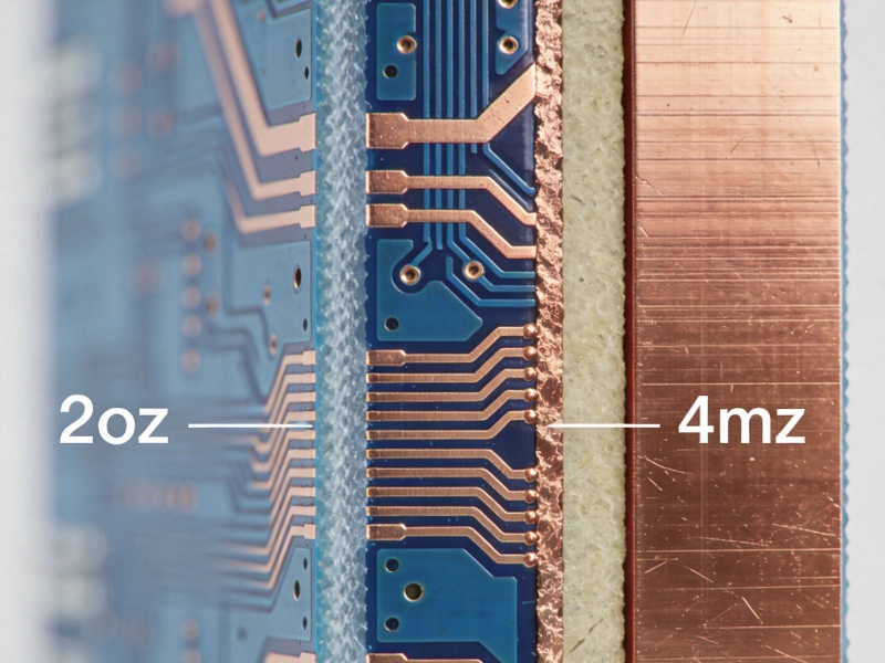
2oz vs. 4oz Copper: Which is Best for Your High Current PCB?July/10/2026

High Current PCB Design for Railway Traction SystemsAugust/07/2026