

Designing a PCB for a high-current audio amplifier presents unique challenges that go beyond standard Pcb Layout practices. Audio amplifiers demand both precise low-level signal handling and robust power delivery, all while maintaining absolute silence—no humming, no buzzing, no RF interference. Ground loops, the most common source of audio noise, are often rooted in Pcb Layout mistakes that are difficult to fix after fabrication. This guide walks through the critical design decisions that determine whether your amplifier sounds pristine or plagued by noise.
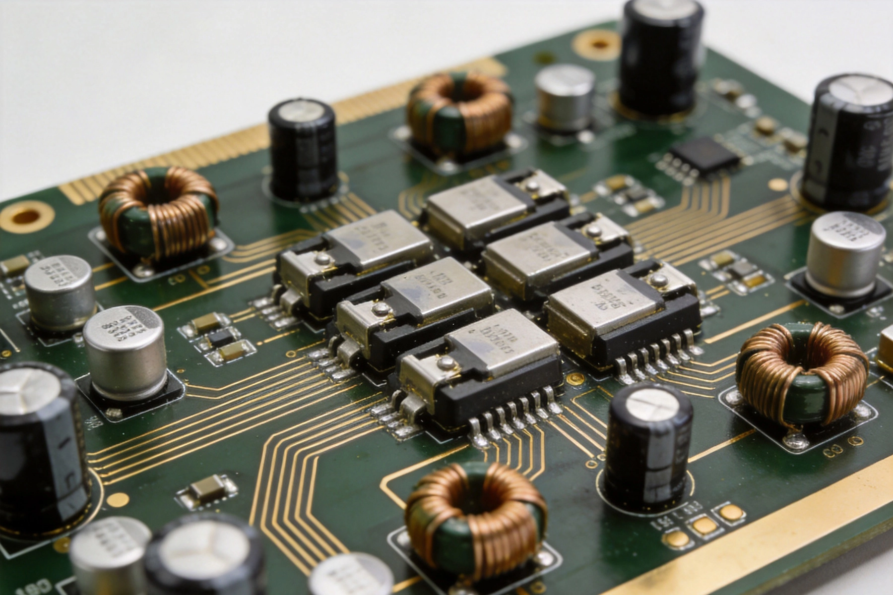
A ground loop occurs when there are multiple paths for return current to flow back to the power supply, creating unintended voltage differences between ground points. In audio circuits, even a few millivolts of ground potential difference between the input and output sections translates directly into audible hum at 50/60 Hz or their harmonics.
Ground loops typically arise from three conditions: shared impedance in ground conductors, magnetic coupling between current loops, and differences in reference potentials between interconnected equipment. On a PCB, the first condition is the most common culprit. When High Current flows through a ground trace that is also used as a reference for low-level signals, the voltage drop across that trace becomes noise injected into the signal path.
The most effective strategy for eliminating ground loops in audio amplifiers is a Star Ground Topology. All ground references—power ground, signal ground, input ground, output ground—connect to a single point, typically near the power supply return. This ensures that high currents do not share conductors with sensitive signal paths.
In practice, this means routing separate ground traces from each functional section directly to the star point, rather than daisy-chaining grounds through the board. The power ground plane handles the high currents from the output stage. The signal ground plane is reserved exclusively for low-level input circuits and analog signal processing. These two planes connect at only one point.
It is tempting to use a single ground plane for everything on a multilayer board, relying on the low impedance of the plane to equalize potentials. While a solid ground plane does reduce impedance, it does not eliminate the problem entirely. Current from the output stage still flows through shared portions of the plane, creating potential differences that can couple into sensitive signal traces nearby.
Audio amplifiers delivering tens to hundreds of watts require substantial copper to carry high currents without excessive heating. The Ipc-2152 standard provides guidance for current-carrying capacity, but audio applications often warrant conservative sizing because thermal rise in the board can affect Component Placement and long-term reliability.
A good rule of thumb for class-AB amplifiers: allocate approximately 20 mils of trace width per ampere for external traces on standard 1 oz copper. For a 50-watt per channel stereo amplifier running on 35V rails, peak output current can exceed 3 amperes per channel. That means power traces to and from the output transistors should be at least 60 mils wide, and ground traces carrying both channels should be proportionally wider.
For extreme high-current designs, consider Heavy Copper layers—2 oz or even 3 oz copper—or dedicated bus bars integrated into the PCB stack-up. Thermal relief spokes connecting SMD components to Heavy Copper planes help with solderability while still providing current capacity.
Physical separation of power and signal sections on the board reduces magnetic coupling and prevents high-frequency switching noise from the power stage bleeding into the audio path. Place the input jacks, volume control, and preamp circuitry in one corner of the board. Locate the output stage and power supply filtering in the opposite corner or on a separate section.
Between these sections, maintain a clear boundary. Route control lines and power connections with care, avoiding runs that pass directly across the boundary carrying noise-sensitive signals. When a signal must cross from the input section to the output section—say, for a feedback path from the output back to the input stage—use a differential pair or a carefully shielded single-ended trace with ground guard rings on either side.
Audio amplifiers are sensitive to power supply noise. The output stage draws current in large, fast pulses as it reproduces the audio waveform. These current pulses can modulate the power supply voltage, injecting noise that appears at the output. Decoupling capacitors placed close to the power pins of each active device absorb these pulses and filter high-frequency noise.
Use a combination of bulk capacitance—typically 1000 µF to 4700 µF electrolytic per watt of output power—and local ceramic decoupling—100 nF to 1 µF MLCCs placed within 5 mm of each power pin. The ceramics handle high-frequency transients that the electrolytics cannot respond to quickly enough.
For the input and preamp stages, consider dedicated low-noise voltage regulation. Even if the main supply is adequately filtered, separate regulation for the preamp stage provides an additional barrier against power supply noise. Low-dropout regulators with high PSRR (power supply rejection ratio) ratings are appropriate here.
Component Placement directly affects the quality of the ground layout. Place input and output connectors on opposite sides of the board if possible, forcing signal flow in a logical path from input to output without crossing itself. Keep the input circuitry away from the output stage and its heat-generating output transistors.
Route low-level signal traces on internal layers surrounded by ground planes above and below, providing shielding from external noise and from the high-current traces on the outer layers. If using a two-layer board, route critical signal traces with adjacent ground traces on either side, creating a microstrip transmission line with controlled impedance and reduced susceptibility to external fields.
Avoid 90-degree bends on high-speed or high-current traces. Mitered corners or rounded traces reduce inductance and prevent current bunching at sharp corners. For the high-current output traces, the difference is minor, but for the signal traces feeding the input stage, clean routing reduces parasitics.
High-current audio amplifiers generate significant heat in the output stage. Junction temperatures above 150°C degrade reliability and can shift bias points in class-AB designs, increasing distortion. Effective Thermal Management starts with the PCB layout.
Use Thermal Vias extensively under output transistors and power regulators to conduct heat from the component side to internal or bottom-side copper planes. The more copper connected to a heat-generating device, the lower its thermal resistance to ambient. Large copper pads under DPAK, TO-220, and similar packages improve thermal performance substantially.
Consider using metal-core PCB or aluminum-backed substrates for very high-power designs. These substrates conduct heat more effectively than standard FR-4 and allow higher power dissipation in the same footprint. The trade-off is increased cost and reduced flexibility in layer count.
Keep temperature-sensitive components—precision resistors, film capacitors, op-amps in the signal path—away from heat sources. The preamp stage should be positioned where airflow or conduction from the PCB can keep it cool. Thermal simulation tools can identify hot spots before the board is fabricated, allowing layout adjustments that would be impossible to implement post-production.
Class-D amplifiers, which switch at frequencies of 300 kHz to 1 MHz, present additional EMI challenges. The high-speed switching transitions generate broadband noise that can interfere with AM radio reception and radiate through the power supply lines. Shielding Cans over the switching section, or a full board-level shield partition, contain this radiation.
For class-D designs, place the LC output filter—typically an inductor and capacitor—close to the output connector to minimize the loop area of the filter section. A compact filter layout reduces both radiated and conducted emissions.
After assembly, test the amplifier with a low-distortion signal source and analyze the output spectrum with an FFT analyzer. Any hum at 50/60 Hz or harmonics indicates a ground loop or insufficient power supply filtering. Inject a test signal and measure the noise floor with the input terminated to ground to isolate the amplifier's intrinsic noise from externally coupled interference.
If hum appears, systematically disconnect sections of the board to isolate the source. Check for shared ground paths between input and output, verify decoupling capacitor placement, and inspect for unintended ground loops in the chassis wiring if the board is housed in an enclosure.
Before sending your design to fabrication, verify that the following items are addressed: star ground point defined with single connection between signal and power grounds; high-current traces sized per current requirements with appropriate Copper Weight; separate physical zones for input, preamp, and output stages; decoupling capacitors placed within 5 mm of every power pin; low-level signal traces routed on shielded layers away from high-current paths; thermal relief and vias under heat-generating components; and Emi Filtering and shielding planned for class-D switching circuits.
A well-designed audio amplifier PCB is not just a matter of connecting components. It is a careful balancing act between power delivery and signal integrity, between Thermal Management and component placement, between shielding and accessibility. Get the layout right the first time, and your amplifier will deliver clean, quiet audio performance for years.
High Current PCB Design for Electric Vehicle Charging StationsAugust/15/2026
Designing a High Current PCB Motor Driver: Avoiding EMI PitfallsJuly/14/2026
Plated Through Hole Current Rating: Complete Guide for PCB DesignersMay/21/2026
Designing a 100A High Current PCB for EV Battery Management SystemsJuly/09/2026
5 Critical Thermal Management Problems in High Power PCBsMay/21/2026
High Current PCB Design Guidelines: Ensuring Reliability and SafetyJune/08/2026
High Current PCB Design for Uninterruptible Power Supplies (UPS)September/02/2026
High Current PCB Design for High-Power LED DriversAugust/12/2026