

Medical imaging equipment represents one of the most demanding applications for High Current printed circuit board (PCB) design, requiring exceptional reliability, precision, and safety in environments where component failure can have life-critical consequences. From magnetic resonance imaging (MRI) and computed tomography (CT) scanners to ultrasound machines and digital X-ray systems, medical imaging equipment demands PCBs that handle substantial currents while maintaining Signal Integrity, thermal performance, and regulatory compliance. This comprehensive guide explores the specialized requirements, design considerations, and best practices for developing High Current PCBs that meet the rigorous standards of medical imaging applications.
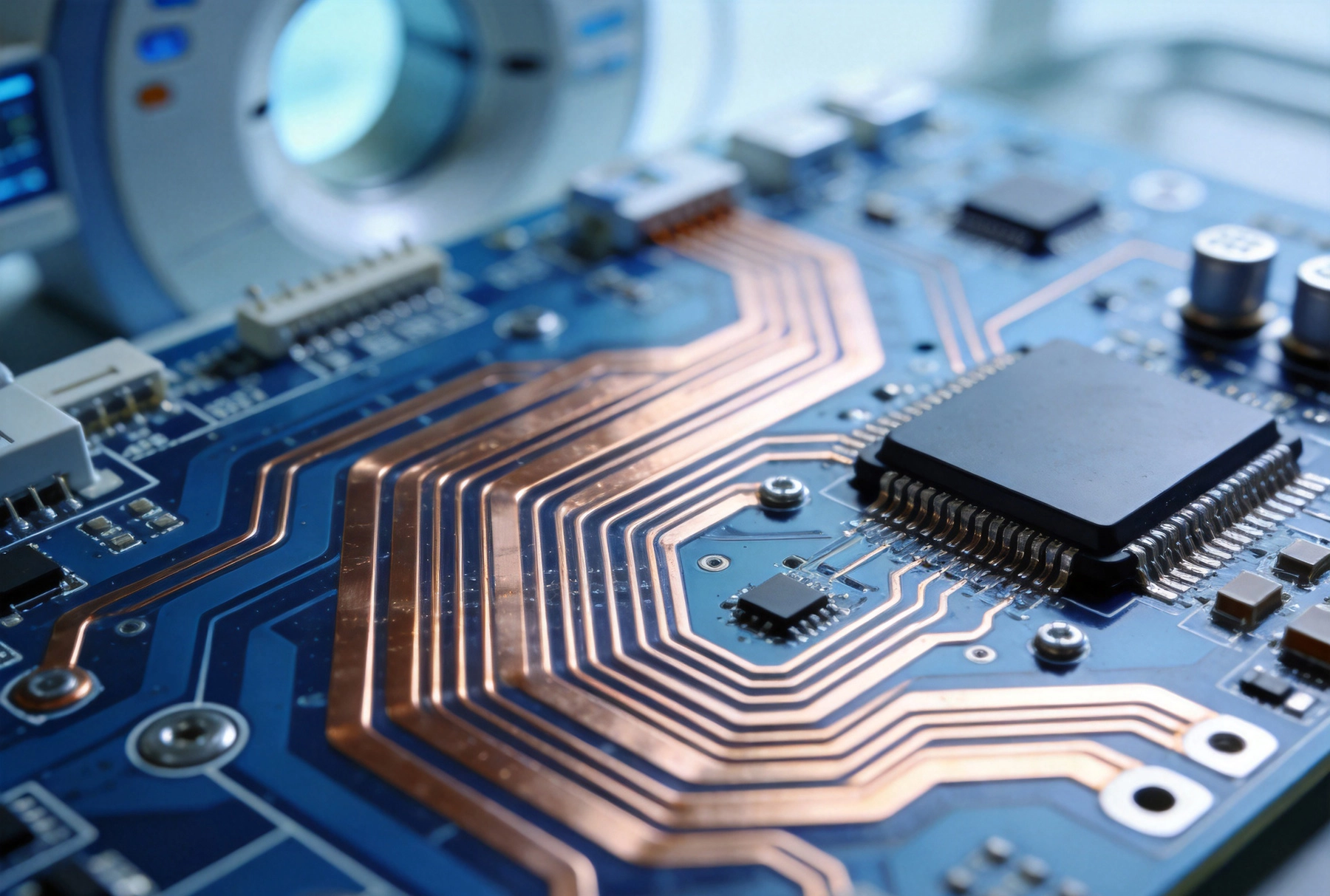
Medical imaging equipment imposes unique design requirements that distinguish it from other high current applications. The primary distinction lies in the critical nature of reliability and safety—where industrial equipment failures cause production delays, medical equipment failures can potentially endanger patient health. This fundamental difference elevates every aspect of Pcb Design, from component selection and Copper Thickness to Thermal Management and safety compliance. Medical imaging PCBs must operate reliably for extended periods often exceeding 10 years of continuous service, with maintenance windows occurring only during scheduled downtime rather than as-needed repairs.
Signal Integrity requirements in medical imaging equipment demand exceptional Pcb Design capabilities. Medical imaging systems process extremely low-level signals from sensors and detectors that require minimal noise interference while simultaneously handling high currents for Power Distribution, motor control, and electromagnet operation. This coexistence of sensitive analog signals and substantial power currents on the same PCB board creates complex electromagnetic interference (Emi) challenges that must be addressed through careful layout design, grounding strategies, and shielding techniques. The PCB must provide both high current capability and low noise signal routing without compromising either requirement.
Regulatory compliance represents another critical differentiator for medical imaging PCBs. All medical electronic equipment must comply with international safety standards, most notably IEC 60601 for medical electrical equipment, which establishes comprehensive requirements for patient safety, electrical isolation, leakage current, and electromagnetic compatibility. Achieving compliance with these standards requires incorporating specific design features such as reinforced insulation, Creepage And Clearance distances, and isolation barriers directly into the PCB design. Unlike other applications where safety features might be added as afterthoughts, medical PCBs must integrate safety compliance from the initial design concept through final manufacturing.
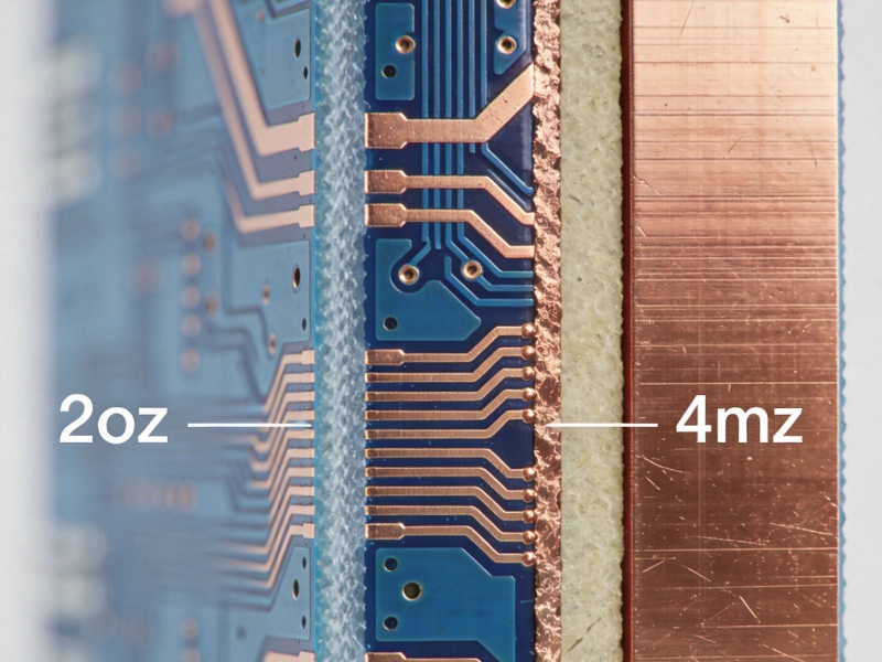
Selecting appropriate Copper Thickness represents the foundation of High Current PCB design for medical imaging equipment. While standard PCBs typically use 1 oz (35 μm) copper thickness, medical imaging applications frequently require copper thicknesses ranging from 2 oz (70 μm) to 6 oz (210 μm) or more, depending on specific current requirements and thermal considerations. Heavy Copper traces provide lower resistance, reduced voltage drop, and improved thermal performance, all critical for medical imaging systems where precision and reliability cannot be compromised. The selection process involves calculating required Current Carrying Capacity based on load specifications, acceptable temperature rise, and ambient operating conditions.
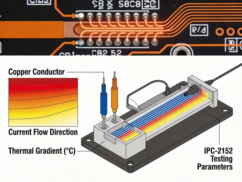
The relationship between copper thickness and Current Carrying Capacity follows well-established design guidelines such as Ipc-2221, which provides formulas and charts for determining appropriate trace width and thickness based on current requirements and acceptable temperature rise. However, medical imaging applications often require more conservative designs than the minimum specifications established by these standards. Designers typically apply safety factors of 1.5 to 2.0 times the calculated minimum requirements to account for manufacturing variations, aging effects, and unexpected operating conditions. This conservative approach ensures that PCBs maintain adequate current carrying capacity throughout their service life even under worst-case conditions.
Copper thickness uniformity across the PCB becomes particularly important for medical imaging applications where thermal gradients can affect system performance. Non-uniform copper thickness creates varying resistance and thermal characteristics across the board, potentially causing thermal hot spots or affecting signal integrity in critical analog circuits. High-quality fabrication processes with strict thickness control specifications (typically ±10% or better) are essential for medical imaging PCBs. Designers should work closely with PCB manufacturers to establish appropriate copper thickness specifications and quality control procedures that ensure consistent performance across production batches.
Effective Thermal Management represents one of the most critical aspects of High Current PCB design for medical imaging equipment. The substantial currents flowing through Pcb Traces generate significant heat that must be dissipated effectively to maintain component reliability and performance. Inadequate thermal management leads to elevated operating temperatures that accelerate component aging, reduce reliability, and potentially cause premature failures—unacceptable consequences in medical imaging applications where equipment availability directly impacts patient care.
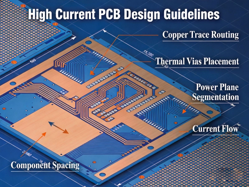
Copper planes play a central role in thermal management for medical imaging PCBs. Large copper areas provide efficient heat spreading capabilities, distributing heat from concentrated heat sources across the entire board surface area where it can be dissipated more effectively. Designers strategically place copper planes not only for Power Distribution and grounding but also for thermal management purposes, often incorporating multiple copper layers connected through Thermal Vias to create three-dimensional heat spreading structures. The size and location of thermal planes are carefully planned based on thermal simulation results and component power dissipation characteristics to ensure optimal thermal performance.
Thermal Vias enable effective heat transfer between copper layers, creating vertical thermal pathways that connect heat-generating components to larger copper planes on other layers or to the opposite side of the board where heat can be dissipated more effectively. In high current medical imaging PCBs, thermal via arrays become essential components of the thermal management strategy, particularly under power semiconductors, voltage regulators, and other components generating substantial heat. Designers specify thermal via fill with conductive epoxy or solder to enhance thermal conductivity, ensuring maximum heat transfer capability through the via structures.
External thermal management interfaces integrated directly into the PCB design provide additional Heat Dissipation capabilities. Medical imaging systems often incorporate thermal interface materials, Heat Sinks, and active cooling systems that connect directly to the PCB. Designers integrate mounting features, Thermal Pad surfaces, and connection points for these external cooling systems directly into the Pcb Layout, ensuring efficient thermal coupling between the PCB and the cooling system. Careful consideration of thermal interface material properties, surface flatness requirements, and mechanical mounting arrangements ensures reliable thermal performance throughout the equipment's operational life.
Safety compliance represents the most critical non-functional requirement for medical imaging PCBs, with IEC 60601 establishing comprehensive standards for medical electrical equipment safety. This standard addresses multiple safety aspects including electrical insulation, leakage current limits, grounding and bonding, electromagnetic compatibility, and mechanical safety. PCB designers must incorporate these requirements directly into the board layout rather than relying on external measures, ensuring that the PCB itself contributes to overall equipment safety rather than introducing potential hazards.
Electrical isolation requirements in IEC 60601 mandate specific Creepage And Clearance distances between conductive parts at different voltage levels, particularly between patient-connected circuits and other parts of the equipment. PCB designers must ensure adequate spacing between traces and components based on the voltage differentials and pollution degree ratings specified in the standard. For high current medical imaging PCBs operating at elevated voltages, these spacing requirements can become significant design constraints, requiring careful layout optimization and potentially additional PCB layers to accommodate required clearances without compromising performance or manufacturability.
Leakage current limits established by IEC 60601 restrict the amount of current that can flow from accessible conductive parts to earth ground or between different parts of the equipment. High current PCBs, with their substantial power distribution networks and potential for capacitive coupling, represent significant leakage current sources. Designers implement specific measures to control leakage currents including isolation transformers, guard traces, creepage and clearance optimization, and careful selection of insulation materials. These measures must be incorporated into the PCB design from the earliest stages, as retrofitting leakage current controls after the initial design is complete often proves difficult and ineffective.
Patient protection circuits integrated into the PCB provide essential safety functions for medical imaging equipment. These circuits include isolation barriers, overcurrent protection, voltage monitoring, and ground fault detection systems that protect patients from electrical hazards during imaging procedures. Designers implement these protection circuits using components specifically rated for medical applications, incorporating redundancy where required and ensuring that protection circuits remain functional under fault conditions. The placement and routing of protection circuitry requires careful consideration to maintain integrity while also providing accessibility for testing and calibration during equipment maintenance.
The power distribution architecture represents the backbone of high current medical imaging PCBs, determining how electrical power reaches various subsystems while maintaining reliability and safety. Medical imaging systems typically require multiple voltage rails with different current capabilities, ranging from low-voltage low-current supplies for digital electronics to high-voltage high-current supplies for electromagnets, X-ray tubes, and motor drives. Designing an efficient power distribution architecture involves analyzing power requirements, establishing appropriate distribution topology, and implementing protection and monitoring systems.
Multi-layer power distribution architectures optimize performance by dedicating specific PCB layers to different voltage rails or power distribution functions. This approach reduces voltage drop, minimizes electromagnetic interference, and simplifies routing of power traces while maintaining adequate current carrying capacity. For medical imaging PCBs, designers might dedicate inner layers to high current power distribution with large copper areas and multiple vias for current sharing, while using outer layers for lower Current Distribution and signal routing. The Layer Stackup must accommodate these distribution requirements while also providing adequate copper thickness, dielectric materials, and impedance control for signal integrity requirements.
Decoupling Capacitor placement and sizing directly affects power distribution quality in medical imaging systems. High current applications generate significant switching noise and transient currents that can affect sensitive imaging electronics if not properly decoupled. Designers implement hierarchical decoupling strategies, placing bulk capacitors near power entry points, intermediate decoupling capacitors distributed throughout the board, and local decoupling capacitors adjacent to each integrated circuit. The capacitor values, types, and placement locations are carefully optimized based on frequency response characteristics, current loop areas, and physical layout constraints to achieve optimal power distribution quality.
Current sharing across parallel paths becomes an important consideration when distributing high currents through multiple PCB layers or parallel traces. In medical imaging PCBs where current requirements may exceed the capacity of a single trace or layer, designers implement parallel current paths that share the total current load. However, achieving equal current sharing requires careful attention to trace resistance matching, thermal effects, and connection geometry. Slight differences in trace length, width, or copper thickness can cause uneven current sharing, potentially overloading some paths while underutilizing others. Designers use parallel vias, matched trace geometries, and symmetrical layouts to promote balanced Current Distribution across parallel paths.
Signal integrity represents a critical design consideration for medical imaging PCBs, particularly when high current power circuits coexist with sensitive analog signal processing electronics. Medical imaging systems often process extremely low-level signals from sensors, detectors, and analog front-end circuits that require minimal noise interference for accurate image reconstruction. Simultaneously, the high currents required for electromagnets, motors, and X-ray generation create substantial electromagnetic interference that must be prevented from contaminating sensitive signal paths. Managing this coexistence requires careful Pcb Layout, grounding strategies, and filtering approaches.
Grounding architecture plays a fundamental role in noise control for medical imaging PCBs. Designers implement star grounding or hybrid grounding schemes that separate different circuit domains—such as digital, analog, power, and safety grounds—at their source points while maintaining appropriate connections at a single reference point. This approach prevents ground loops that can couple noise between different circuit sections while maintaining proper reference potentials. The grounding system must accommodate both safety requirements, such as protective earth connections, and performance requirements, such as low-impedance returns for high current paths and clean references for analog circuits.
Shielding techniques protect sensitive circuits from electromagnetic interference generated by high current switching and conduction. Medical imaging PCBs often incorporate copper Shielding Cans, guard traces, and dedicated shield layers to isolate noisy power circuits from sensitive analog electronics. Shield effectiveness depends on proper design and implementation, including appropriate grounding of shield structures, minimizing apertures, and ensuring complete coverage of protected circuits. Designers must balance shielding effectiveness with practical considerations such as component accessibility, thermal performance, and manufacturing complexity to achieve optimal noise control without creating new problems.
Filter design and placement reduce conducted and radiated noise at critical points in the circuit. Medical imaging PCBs incorporate various filtering techniques including differential filters for sensitive analog inputs, common-mode chokes for I/O interfaces, and pi filters for power distribution lines. Filter placement follows specific rules—filters are placed as close as possible to noise sources on the noise side and as close as possible to sensitive circuits on the victim side to minimize coupling between filtered and unfiltered sections. The filter component values, types, and physical layouts are optimized based on frequency response requirements, impedance matching considerations, and available board space.
Component selection for medical imaging PCBs extends beyond basic electrical specifications to include reliability, regulatory compliance, and service life considerations. Medical imaging applications demand components specifically rated for medical equipment or at least industrial-grade components with proven reliability records. Consumer-grade components, regardless of their electrical performance, are generally inappropriate for medical imaging equipment due to their limited service life, reduced reliability, and potential safety issues. Designers work with component manufacturers to select parts with appropriate quality ratings, Reliability Data, and documentation support for medical applications.
Power semiconductors including MOSFETs, IGBTs, and power diodes represent critical components in high current medical imaging PCBs, particularly for motor drives, power supplies, and switching circuits. These components must handle substantial currents and voltages while maintaining efficiency and reliability. Designers select power semiconductors based on current carrying capacity, voltage ratings, switching characteristics, and thermal performance, with particular attention to safe operating area (SOA) specifications and current derating requirements. Thermal interface materials, mounting hardware, and heat sinking arrangements for power semiconductors are designed to maintain junction temperatures within specified limits under worst-case operating conditions.
Passive component selection including resistors, capacitors, and inductors must account for high current stress and potential temperature elevations. Standard surface-mount resistors may not be adequate for high current applications, potentially requiring specialized high-power resistor packages or through-hole components with appropriate power ratings. Capacitors used in high current applications must handle ripple currents without excessive internal heating that degrades reliability. Inductors and transformers require careful design or selection to achieve appropriate inductance values, current handling capability, and thermal performance while maintaining physical size compatible with board layout constraints.
Component Placement strategies for medical imaging PCBs prioritize thermal management, electrical performance, and serviceability. High-heat-generating components are placed in locations where thermal management features can effectively dissipate heat without affecting sensitive components. Sensitive analog circuits are positioned away from high current switching nodes and power distribution networks to minimize electromagnetic interference. Components requiring maintenance or calibration are placed in accessible locations that facilitate service activities without requiring complete board removal or extensive disassembly. These placement considerations are integrated with routing requirements and board size constraints to achieve an optimal overall layout.
Manufacturing quality represents a critical aspect of medical imaging PCB production, as defects or inconsistencies can compromise equipment reliability and patient safety. Medical imaging PCB manufacturers must implement comprehensive quality management systems compliant with ISO 13485, the international standard for medical device quality management systems. These quality systems encompass design control, supplier management, process validation, traceability, and risk management—all essential aspects of producing reliable PCBs for medical applications.
Process controls for Heavy Copper PCBs differ significantly from standard Pcb Manufacturing processes due to the increased copper thickness and specialized processing requirements. Heavy copper etching requires longer processing times and different chemical compositions to achieve adequate copper removal without excessive undercut. Via formation in heavy copper boards demands specialized drilling and plating processes to ensure reliable interlayer connections. Manufacturers establish specific process parameters, inspection criteria, and acceptance limits for heavy copper PCBs that differ from standard PCB specifications to ensure consistent quality and performance.
Inspection and testing protocols for medical imaging PCBs provide comprehensive verification of manufacturing quality and performance characteristics. Automated optical inspection (AOI) systems verify correct Component Placement, solder joint quality, and trace integrity. Electrical testing including continuity, isolation, and high potential (hipot) testing verifies electrical performance and safety compliance. Dimensional inspection ensures that boards meet specified tolerances critical for mechanical fit and alignment within equipment assemblies. For high current boards, additional testing including thermal imaging under load conditions may verify thermal performance characteristics.
Documentation and traceability requirements for medical imaging PCBs exceed those for standard commercial applications. Each production batch must include comprehensive documentation including material certifications, process records, inspection results, and test data. Traceability requirements may mandate tracking of specific components to their manufacturing lots and sources, enabling rapid identification and resolution of any component-related issues that arise during equipment service life. This comprehensive documentation provides essential support for regulatory compliance, quality improvement, and field service activities.
Medical imaging technology continues advancing rapidly, driving new requirements and capabilities in PCB design. Emerging imaging modalities including functional MRI, molecular imaging, and portable ultrasound systems create new design challenges and opportunities. These advances often require higher performance, greater miniaturization, and enhanced integration between electronics and imaging systems—all factors that influence PCB design approaches and requirements.
Packaging technology innovations enable closer integration of imaging sensors with PCB electronics, reducing interconnection lengths and improving signal integrity. Wafer-level packaging, chip-on-board assembly, and system-in-package technologies bring detector and sensor elements closer to their associated signal processing electronics, minimizing signal degradation and noise pickup. These packaging approaches introduce new PCB design considerations including thermal management of closely spaced components, specialized assembly processes, and potential redesign of traditional PCB architectures to accommodate more integrated assemblies.
Advanced materials including high-performance laminates, conductive adhesives, and thermal interface materials expand design possibilities for medical imaging PCBs. High-frequency laminates enable improved signal integrity for high-speed digital imaging systems while also providing better thermal characteristics. Conductive adhesives and thermal interface materials with enhanced thermal conductivity improve Heat Dissipation from heat-generating components to PCB copper planes and external cooling systems. These material advances enable higher power densities and improved performance while maintaining or reducing physical size requirements.
Digital integration trends increasingly move analog signal processing functions into digital domains, changing PCB design requirements and approaches. Digital signal processing, field-programmable gate arrays (FPGAs), and application-specific integrated circuits (ASICs) replace traditional analog processing circuits in many imaging systems, shifting design emphasis toward digital routing, clock distribution, and high-speed interfaces rather than analog signal integrity. However, the fundamental requirements for reliable high current power distribution, effective thermal management, and safety compliance remain unchanged, requiring designers to integrate digital capabilities while maintaining established PCB design principles for medical imaging applications.
High Current Pcb Design for medical imaging equipment represents one of the most demanding and rewarding challenges in electronics design. The combination of substantial power requirements, exceptional reliability needs, stringent safety standards, and precision performance requirements creates a design problem that demands expertise across multiple disciplines including Electrical Engineering, thermal management, materials science, and regulatory compliance. Successful medical imaging PCBs result from careful attention to every aspect of design—from component selection and copper thickness through thermal management and safety compliance.
The fundamental principle guiding medical imaging PCB design centers on reliability and safety above all other considerations. While performance optimization, cost reduction, and size minimization remain important objectives, these goals must never compromise the fundamental requirements for safe, reliable operation throughout extended service lives under demanding conditions. Designers who prioritize reliability and safety while still achieving performance and efficiency goals create medical imaging PCBs that serve patients effectively while meeting regulatory requirements and delivering value to healthcare providers.
As medical imaging technology continues advancing, PCB design approaches must evolve accordingly to support new capabilities, higher performance, and improved patient care. However, the fundamental principles of reliability, safety, and quality that define excellence in medical imaging PCB design remain constant regardless of technological advances. Designers who master these fundamental principles while embracing new technologies and approaches will be well-positioned to meet the evolving challenges of medical imaging electronics and contribute to continued advances in healthcare technology that improve patient outcomes and save lives.
Designing a High Current PCB Motor Driver: Avoiding EMI PitfallsJuly/14/2026
Designing a 100A High Current PCB for EV Battery Management SystemsJuly/09/2026
High Current PCB Design for High-Frequency Switching RegulatorsSeptember/04/2026
2oz vs. 4oz Copper: Which is Best for Your High Current PCB?July/10/2026
High Current PCB Design for Data Center Power ShelvesOctober/19/2026
High Current PCB Design GuidelinesMay/21/2026
IPC-2152 Current Carrying Capacity Calculation GuideJune/03/2026
High Current PCB Pad Design: Reinforced Plating vs. Standard PadsJuly/28/2026