

Designing a PCB for a high-power microwave generator is a fundamentally different challenge than laying out a typical digital control board. When you are dealing with currents that can reach tens or even hundreds of amperes while simultaneously managing microwave frequency signals, the design rules change dramatically. A layout that would work fine for a low-power microcontroller application will fail catastrophically when asked to carry High Current alongside sensitive RF paths. Understanding these differences before you start your design will save you from expensive revisions and field failures.
This article walks through the critical design considerations for PCBs handling High Current in microwave generator applications. The goal is to help engineers and product designers make informed decisions about material selection, Trace Geometry, Thermal Management, and manufacturing requirements so that the finished board performs reliably in demanding environments.

High-power microwave generators present a unique design challenge because they simultaneously demand high Current Carrying Capacity and microwave frequency Signal Integrity. These two requirements often pull design decisions in different directions, and navigating that tension is what separates successful designs from problematic ones.
At high currents, your primary concerns are Thermal Management and electromigration resistance. Current flowing through a conductor generates heat according to power equals current squared times resistance. When currents reach tens of amperes, even small resistances produce meaningful heat that must be dissipated or conducted away. Left unchecked, this heat leads to trace degradation, solder joint failures, and ultimately board failure.
At microwave frequencies, your primary concerns shift to impedance control, skin effect, and Signal Integrity. At frequencies above approximately 1 GHz, current tends to flow near the surface of conductors rather than uniformly through the cross-section. This skin effect reduces effective conductor area, increasing resistance and changing the electrical characteristics of your transmission lines in ways that simple DC current calculations cannot predict.
The designer must account for both regimes simultaneously. A trace that is wide enough to carry the required current at DC may not maintain the correct impedance at microwave frequencies. A transmission line with perfect high-frequency characteristics may overheat if it cannot dissipate the real power being delivered. Getting both right requires careful attention to multiple design parameters.
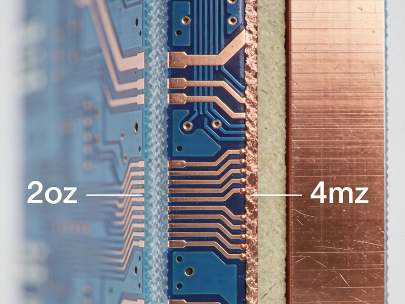
The most straightforward way to increase Current Carrying Capacity is to use heavier copper. Standard PCB Fabrication typically uses 1 ounce per square foot copper, which is approximately 35 microns thick. For high current applications, 2 ounce, 3 ounce, or even heavier copper is often necessary to keep trace temperatures within acceptable limits.
Heavier copper does not simply scale Trace Current Capacity linearly. The relationship between Copper Weight and current capacity is complex because Heat Dissipation depends on Trace Geometry, surrounding materials, airflow, and the thermal properties of the board substrate. However, as a general rule, doubling Copper Weight approximately doubles the current a given trace can carry before reaching a target temperature rise.
Manufacturing constraints limit how heavy you can go. Standard PCB Fabrication processes can reliably produce boards with copper weights up to 3 or 4 ounces. Beyond that, special processing is required, and not all manufacturers can handle very Heavy Copper. If your design requires extremely high current, you may need to consider thick copper bus bars attached to the PCB or even Bus Bar construction where the PCB is eliminated entirely for current-carrying sections.
Heavier copper also affects other design parameters. Etching heavier copper takes longer and may produce less precise sidewall angles, affecting impedance control. Via formation becomes more challenging because plating time must increase to achieve adequate barrel thickness. These manufacturing realities need to be communicated to your fabricator early in the design process.
Once you have selected your copper weight, calculating appropriate trace widths requires understanding both the current you need to carry and the acceptable temperature rise for your application. Various online calculators and IPC standards provide starting points, but the real-world performance of your board will depend on your specific thermal environment.
For internal traces, where Heat Dissipation is more difficult, wider traces are required for the same current compared to surface traces. A trace on the outer layers can dissipate heat to the surrounding air and radiate to nearby surfaces. An internal trace has only conduction paths through the substrate material, which is typically a poor thermal conductor. This means internal high-current traces often need to be two to three times wider than surface traces carrying the same current.
Temperature rise targets vary by application. For consumer electronics where some warming is acceptable, allowing a 20 to 30 degree Celsius rise above ambient is common. For high-reliability applications, you may want to limit temperature rise to 10 degrees or less, which requires significantly wider traces or alternative cooling strategies.
Slotting and cutouts offer ways to increase effective trace width without consuming additional board area. By creating elongated slots in the copper plane adjacent to your current path, you can concentrate current in wider individual conductors while maintaining the overall routing channel width. This technique requires careful analysis because slots can create impedance discontinuities and field concentration effects that affect high-frequency performance.
Trace width alone is often insufficient for managing heat in high-power microwave generators. Additional thermal management strategies are typically required to keep temperatures within acceptable limits and ensure long-term reliability.
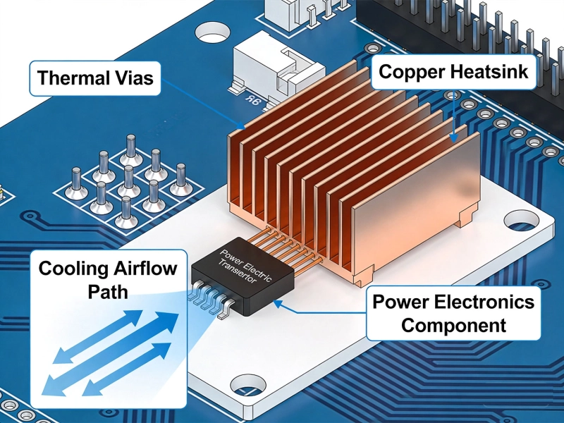
Thermal Vias provide a path for heat to travel from hot components or traces to other layers of the board or to external heatsinking. For high-current applications, Thermal Vias should be placed strategically under current-carrying traces and under components that dissipate significant power. The via pattern, size, and plating thickness all affect thermal conductivity. Heavily plated thermal vias can dramatically reduce Thermal Resistance between board layers.
Metal core substrates offer another approach to thermal management. A Metal Core Pcb has an aluminum or copper core that acts as a thermal spreading layer, distributing heat across a larger area before it must be dissipated to the environment. Metal core boards are more expensive than standard substrates but can be essential for high-power designs where surface mount cooling alone is insufficient.
Heatsinking from components extends to the PCB itself. When high-power components like RF transistors or power transistors are mounted on the PCB, their thermal path through the board is critical. Large thermal vias, copper pad areas, and sometimes external heatsink attachments are necessary to keep junction temperatures within rated limits. This is especially important for gallium nitride and silicon carbide transistors commonly used in modern microwave generators, which can generate significant heat per unit area.
Vias present a particular challenge in high-current Pcb Design because they interrupt current flow and create resistance. A via barrel has a certain cross-sectional area for current flow, and when that area is significantly smaller than the trace width, it becomes a current bottleneck and a heat source.
The simplest solution is to use multiple vias in parallel for high-current connections. By spreading current across several smaller vias rather than concentrating it in one large via, you reduce resistance and improve current sharing. The total cross-sectional area of the via array should match or exceed the cross-sectional area of the trace it connects to.
Via barrel plating thickness affects current capacity significantly. Standard plating of 25 microns may be insufficient for high-current vias. Heavy plating options of 35 microns or more provide greater current capacity per via and better thermal conductivity. Some fabricators offer custom plating thickness specifications that can be optimized for your current requirements.
Via-in-pad construction, where vias are placed directly in component pads, is sometimes used to improve thermal and electrical connections for high-power components. This requires careful manufacturing to ensure solder does not wick down the via barrel during assembly, which could create a void under the component. Encapsulating or tenting vias on the opposite side helps prevent this issue.
Standard FR4 substrate works for many high-power applications, but at higher power levels or when microwave frequencies are involved, material selection becomes more critical. The dielectric properties of your substrate affect both electrical performance and thermal management.
For microwave frequencies, the dissipation factor of your substrate material matters. Lower dissipation factor means less signal loss as energy passes through the dielectric. Standard FR4 has a dissipation factor around 0.02 at GHz frequencies, which may be acceptable for some applications but problematic for others. Low-loss substrates like Rogers or Isola materials offer dissipation factors of 0.002 or lower, which can make a meaningful difference in insertion loss and heat generation in the substrate itself.
Thermal conductivity varies significantly between substrate materials. Standard FR4 has thermal conductivity around 0.3 W/mK, while some high-performance substrates offer thermal conductivity of 0.5 W/mK or higher. While these numbers are modest compared to metal, the difference can be meaningful in thermal management calculations for densely packed high-power designs.
Glass transition temperature matters for high-power applications because the board will experience elevated temperatures during operation. FR4 typically has a Tg around 135 to 140 degrees Celsius, which provides some margin above typical operating temperatures but may be insufficient if local heating creates hotspots near maximum ambient conditions. High-Tg materials offer greater thermal margin and better resistance to Thermal Cycling damage.
High-power circuits require exceptional attention to grounding. Poor grounding creates voltage drops, introduces noise into sensitive circuits, and can create safety hazards in extreme cases. For microwave generators operating at hundreds of watts or kilowatts, proper grounding is not optional.
Ground plane integrity is essential.Segmented ground planes create return current paths that must travel longer distances and encounter impedance that affects both circuit performance and electromagnetic emissions. Whenever possible, maintain solid ground planes under high-current traces and under sensitive microwave circuits. Slotting the ground plane to route high-current traces should be done only after careful analysis of how the slots affect return current paths.
Decoupling and bypass strategies become more important at high power levels. The fast transients associated with switching power stages can couple noise into sensitive microwave circuits if decoupling is inadequate. Multiple bypass capacitors of different values, placed strategically, help maintain clean voltage rails throughout the board.
Shielding and enclosure design affect both electromagnetic compatibility and thermal performance. Metal enclosures provide shielding but also create thermal enclosures unless ventilation or active cooling is provided. The interaction between Pcb Layout, shielding design, and thermal management should be considered as an integrated system rather than separate design domains.
High-power PCB designs benefit significantly from thorough testing and validation because the consequences of failure can be severe. A design that works in the lab but fails in the field due to thermal issues or reliability concerns has not truly succeeded.
Thermal imaging during operation reveals hot spots that calculations may not predict accurately. By viewing the board under load with a thermal camera, you can identify traces or components that are running hotter than expected and make targeted improvements. This testing is most valuable when comparing design iterations to validate whether changes actually improve thermal performance.
Long-term reliability testing under accelerated conditions helps identify failure mechanisms that might take months or years to appear in field service. Temperature cycling, high-temperature storage, and power cycling tests can reveal weaknesses in solder joints, trace adhesion, and material degradation before they cause field failures.
Electrical testing at full power validates that the board performs as designed under real operating conditions. This includes measuring voltage drops across current-carrying paths, verifying impedance of transmission lines, and checking for unexpected coupling or interference between circuits. Documentation of these measurements provides a baseline for future comparison and helps diagnose any issues that emerge during service.
Designing PCBs for high-power microwave generators requires balancing multiple competing requirements: current capacity, microwave performance, thermal management, and manufacturing practicality. Success comes from understanding how these factors interact and making informed trade-offs based on your specific application requirements.
Starting with appropriate copper weights, calculating trace widths for your actual thermal environment, and selecting materials that match your frequency and power requirements creates a solid foundation. Adding thoughtful thermal management through vias, heat spreading, and external cooling strategies helps ensure the board can dissipate the heat it generates without degradation. Careful attention to grounding and shielding protects sensitive microwave circuits from noise and interference.
The most successful high-power designs typically involve close collaboration between the electrical designer, the thermal engineer if available, and the PCB fabricator. Early discussion of manufacturing capabilities and constraints prevents surprises during production and ensures the design can be built reliably at the quantities you need.
Contact us to discuss your requirements and explore the right design approach for your high-power microwave generator application.
High Current PCB Design for Industrial Motor DrivesSeptember/28/2026
High Current PCB Design Guidelines: Ensuring Reliability and SafetyJune/08/2026
High Current PCB Design for Telecommunications Base StationsSeptember/18/2026
Designing a High Current PCB for Industrial Welding EquipmentJuly/23/2026
Designing a High Current PCB Motor Driver: Avoiding EMI PitfallsJuly/14/2026
2oz vs. 4oz Copper: Which is Best for Your High Current PCB?July/10/2026
Why Your High-Power PCBs Overheat (And the 5 Methods That Actually Fix It)May/20/2026
High Current PCB Design for Electric Vehicle Charging StationsAugust/15/2026