

Industrial motor drives are among the most demanding applications in Power Electronics. A variable frequency drive (VFD) controlling a 30kW motor might switch hundreds of amps at bus voltages of 400V to 690V, generating heat inIGBT modules, DC link capacitors, and the Pcb Traces that connect them. The PCB is not a passive substrate in these systems — it is an active thermal and electrical element whose design directly determines whether the drive operates reliably for 60,000 hours or fails within the first year of service.
Designing PCBs for High Current motor drive applications requires a different mindset than designing boards for signal-level logic. This article walks through the key design decisions that engineering teams face when laying out a motor drive PCB: trace width and Copper Weight, Thermal Management, Via Current Capacity, layer stack-up, and the testing protocols that validate whether the design will survive in the field.
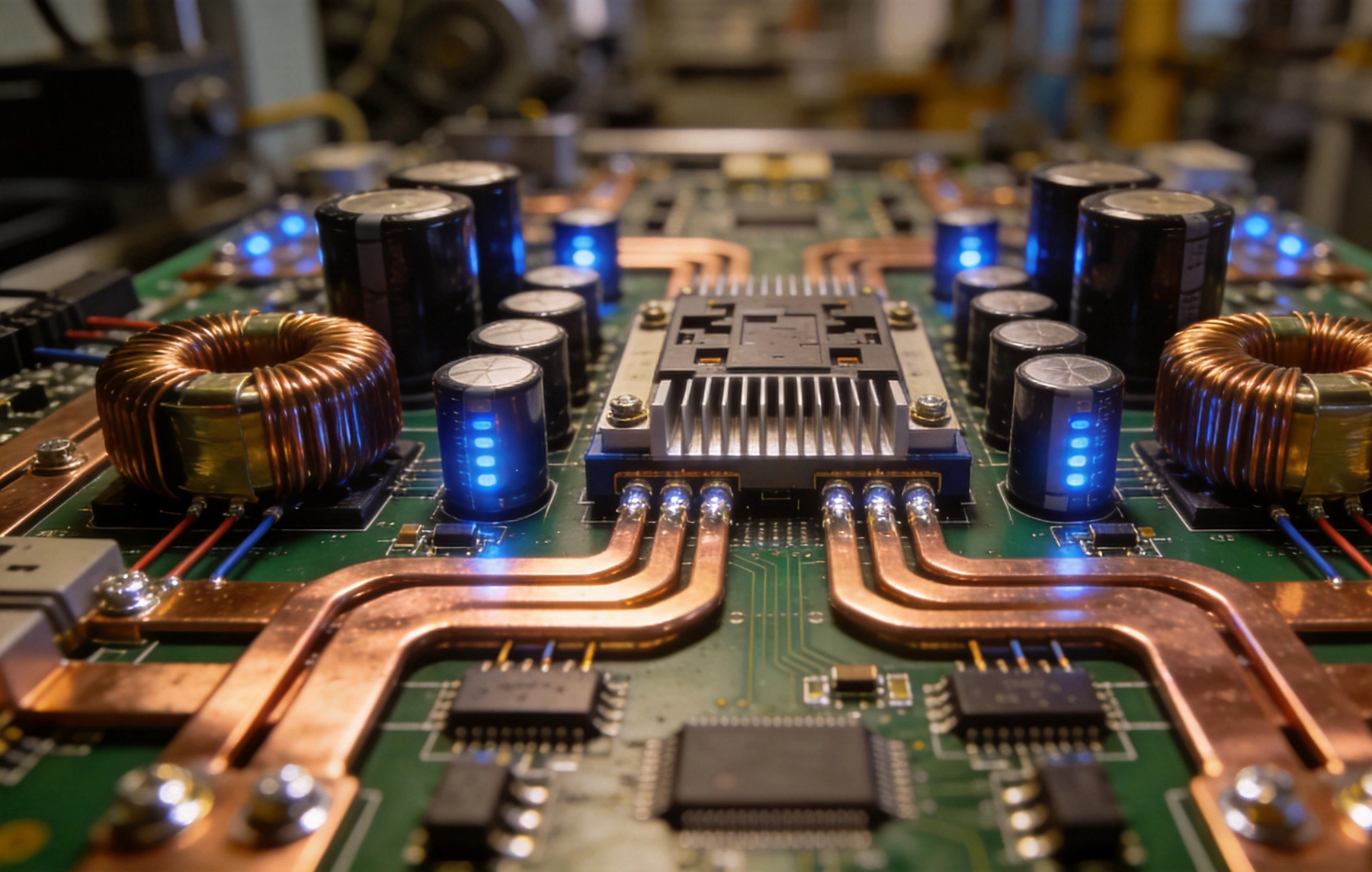
The starting point for any High Current PCB design is accurate Trace Width Calculation. Current Density — measured in amps per millimeter of trace width — determines how much copper cross-sectional area is needed to carry a given current without excessive temperature rise. Exceeding acceptable Current Density causes the trace to heat up, oxidize, and eventually open-circuit.
Ipc-2152 is the standard reference for determining current-carrying capacity in Pcb Traces. Unlike older standards that provided simplified charts, Ipc-2152 accounts for trace width, Copper Weight, board thickness, ambient temperature, whether the trace is enclosed or exposed, and whether it is on an internal or external layer. External traces dissipate heat more effectively to ambient air and can carry roughly 20% to 30% more current than identical internal traces.
For a motor drive PCB carrying 50A on an outer layer with 3oz copper, the required trace width is typically 15mm to 20mm — wide enough that routing becomes a layout challenge. This is why motor drive designs almost universally use copper pours on Power Planes rather than individual traces for High Current paths. A solid copper plane with thermal reliefs connecting to component pads distributes current uniformly and provides a much larger effective cross-sectional area than any single trace.
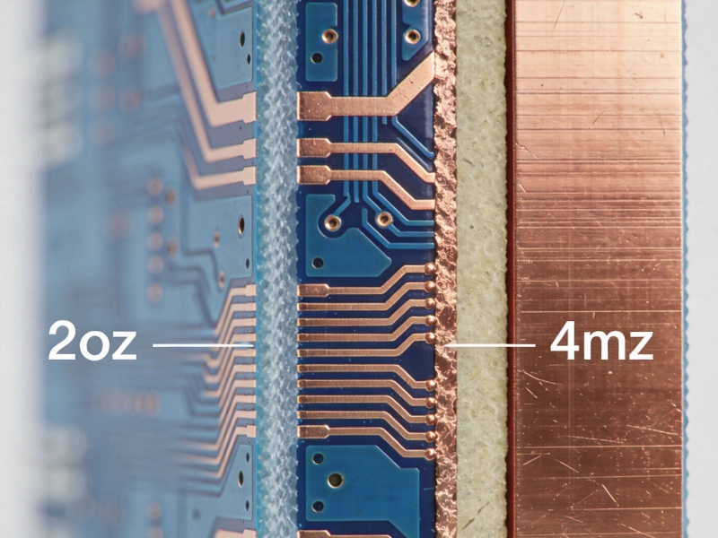
Standard PCB Fabrication uses 1oz copper (35 micrometers) as the default. This is entirely inadequate for motor drive applications carrying more than 10A. For industrial motor drives, 2oz to 4oz copper is typical on outer layers, and 2oz to 3oz on inner Power Planes.
The trade-off is cost and manufacturability. Heavy Copper PCBs require longer etch times, more precise process control, and in some cases special tooling at the fabrication house. Boards with 4oz copper and above also have thicker dielectric layers, which changes the electrical characteristics of the board — particularly important if the motor drive uses PWM switching at high frequencies where stray inductance in the power path matters significantly.
When specifying copper weight, be explicit in your fabrication drawing. Identify each layer by name (e.g., "Layer 1 — Top Power Plane, 3oz copper") rather than relying on a general note. Ambiguity in copper weight specification is one of the most common reasons motor drive designs come back from fabrication with insufficient current-carrying capacity.
Heat is the primary failure mechanism in motor drive PCBs. IGBT and Mosfet Switching losses, resistive heating in the traces and vias, and losses in the DC link capacitors all contribute to board-level temperature rise. If the Pcb Thermal Design does not manage this heat effectively, the temperature at the most stressed point — typically a solder joint or a thermal via under a power semiconductor — can exceed 100°C above ambient, well beyond the safe operating range of most electronic components.
The key Thermal Management strategies for motor drive PCBs include the following.
Thermal Vias under power semiconductors are the primary mechanism for moving heat from the top layer to internal ground planes and ultimately to the board edge or a heatsink. Thermal via arrays should be placed directly under the Thermal Pad of the switching device, with via diameter and spacing calculated to provide low Thermal Resistance path to the nearest heat spreading plane. Typical thermal via arrays use 0.3mm to 0.5mm diameter vias on 0.8mm to 1.2mm pitch, with the array extending over the full Thermal Pad footprint.
Copper pours on multiple layers connected by via stitching create an effective heat spreading structure. A single solid Copper Pour on one layer has limited heat spreading capability. The same copper area distributed across three or four layers and stitched with Thermal Vias creates a thermal plane that can spread heat laterally across a large area and reduce localized temperature peaks significantly.
Metal-backed substrates or IMS (insulated metal substrate) PCBs are used for the highest power sections of motor drives where air cooling alone is insufficient. IMS boards use an aluminum or copper base plate separated from the circuit layer by a thin dielectric with high thermal conductivity. They can move heat from the active components to a heatsink or chassis mounting surface with Thermal Resistance an order of magnitude lower than standard FR4 constructions. The trade-off is higher cost and reduced design flexibility for routing dense signal traces.
Vias in high current paths are often the weakest link in a motor drive PCB. A single via can only carry a limited current before it overheats. The current capacity of a via depends on its diameter, plating thickness, and the thermal resistance between the via barrel and the surrounding dielectric.
As a rough rule of thumb, a standard 0.3mm inner diameter via with 1mil (25 micrometer) plating can carry approximately 0.5A to 1A reliably. For a 50A power path, this means a minimum of 50 to 100 vias in parallel — or larger vias. Many motor drive designs use via-in-plain configurations where a 0.8mm to 1.0mm via carries current directly from a Heavy Copper pad on the top layer to a matching pad on an inner power plane. A 1.0mm diameter via with 1mil plating can carry 3A to 5A under typical conditions.
Slot vias or routed slots are often used for the highest current paths where even a large round via is insufficient. Slots distribute the current path over a wider perimeter than a round via and provide significantly higher current capacity. They are more expensive to fabricate because they require additional routing operations, but for motor drive main current paths carrying 100A or more, they are often the only viable PCB-based solution.
Motor drive PCBs typically have a DC link bus that distributes power from the input rectifier or DC supply to the switching devices. The inductance of this bus is critical: high bus inductance causes voltage overshoot (ringing) at the switching device when it turns off, which stresses the device and generates electromagnetic interference (EMI).
Low-inductance bus design uses wide copper planes for the positive and negative (ground) rails, placed in adjacent layers with minimum dielectric spacing between them. This creates a flat capacitor structure — the two planes separated by the dielectric act as a distributed DC link capacitor, absorbing the high-frequency switching transients before they can radiate or conduct as EMI. The dielectric thickness between the bus planes should be minimized to reduce Loop Inductance. In high-performance motor drives, 0.1mm to 0.2mm prepreg between bus planes is not uncommon.
Decoupling capacitors must be placed as close as physically possible to the switching device pins. For IGBT and MOSFET modules in motor drives, ceramic capacitors (C0G or NP0 type for low ESR at high frequencies) should be within 5mm of the device leads. The trace length from the capacitor to the device pin determines the effective series inductance of the decoupling loop, and every millimeter of Loop Inductance adds to the switching voltage overshoot.
Motor drives operate at high voltages and high currents, but the control circuitry — the gate drivers, the current sensing amplifiers, and the microcontroller — operates at logic-level voltages of 3.3V to 15V. The challenge is routing these low-voltage signal traces across a board that has hundreds of amps and hundreds of volts switching at kilohertz frequencies.
Noise coupling from the power stage into the gate drive and sense circuitry is one of the most common causes of motor drive malfunction. Ground planes under the gate drive section provide a low-impedance return path and reduce inductive coupling of switching noise into the sensitive signal traces. The gate drive traces themselves should be kept short, wide enough to carry the peak gate charge current (typically 1A to 5A pulses), and routed away from high current power traces with at least 5mm separation or a grounded keepout zone between them.
Current sensing in motor drives typically uses shunt resistors or Hall effect sensors to measure phase currents for closed-loop control. Shunt Resistor placement should be on the low-side switching node or phase node, with Kelvin-sense connections routed as a differential pair to the op-amp or current sense amplifier. Kelvin connections ensure that the voltage being measured is the actual shunt voltage, not the voltage drop along the Pcb Trace connecting the shunt to the amplifier.
The PCB laminate material affects both the electrical and thermal performance of a motor drive board. Standard FR4 (Tg 130°C to 140°C) is adequate for low-power drives in controlled environments, but high-power motor drives in industrial settings with ambient temperatures of 40°C to 60°C need higher temperature-rated materials to maintain a safety margin against glass transition.
High-Tg FR4 (Tg 170°C) is the most common choice for industrial motor drives. It costs only slightly more than standard FR4 but provides significantly more margin against delamination and warpage under Thermal Cycling. For the most demanding applications, polyimide (PI) or ceramic-filled substrates provide superior thermal stability and lower Z-axis expansion, which reduces via barrel stress during Thermal Cycling.
The dielectric constant (Dk) and loss factor (Df) of the laminate are less critical for motor drive power sections than for high-frequency RF circuits, but they do matter for the gate drive and PWM signal traces. If the switching frequency exceeds 20kHz, consider using a low-Dk, low-Df material for the signal layers to reduce parasitic capacitance and minimize signal distortion in the gate drive circuits.
Before releasing a motor drive Pcb Design for fabrication, verify the following critical items.
Have you calculated trace widths using IPC-2152 for all current-carrying paths, accounting for layer (internal vs. external), copper weight, and ambient temperature? Use a calculator tool and cross-check manually for paths carrying more than 20A.
Are thermal via arrays placed under all power semiconductor thermal pads with appropriate diameter and pitch for the thermal load? A rule of thumb: the via array should cover at least 60% of the thermal pad footprint with thermal vias on 1.0mm pitch.
Is the DC link bus designed with minimum loop inductance — adjacent positive and negative planes with thin dielectric? Calculate or simulate the bus loop inductance if the switching devices are rated above 600V and switching faster than 10kHz.
Are gate drive traces routed away from high current power traces with ground plane shielding? Gate drive noise coupling is one of the hardest problems to debug in the lab and one of the easiest to prevent with good layout.
Have you specified copper weight explicitly for each layer in the fabrication drawing? Vague copper weight specifications cause boards to come back with inadequate current-carrying capacity.
Does the board material Tg exceed the maximum expected operating temperature by at least 20°C? Include thermal margin for peak load conditions, not just nominal operating conditions.
High current motor drive PCBs should undergo thermal imaging testing under full load to verify that the actual board temperatures match the design expectations. Thermography identifies hotspots that may not have been captured in thermal simulation, particularly at vias and connectors where thermal resistance is difficult to model accurately.
Current injection testing — where a controlled DC current is forced through each high-current path — can identify weak points in the trace and via structure before the full drive system is assembled. Thermal imaging during current injection reveals which vias are overheating and whether solder joints on heavy copper pads have adequate fillet and thermal contact.
Thermal cycling testing to IPC-9701 or equivalent standards validates that the board survives the mechanical stress of repeated heating and cooling. Motor drive PCBs in industrial environments experience thermal cycles every time the motor starts and stops, and the cumulative fatigue on vias, plated through-holes, and solder joints determines the useful lifetime of the assembly.
There is no single answer — it depends on trace width, copper weight, whether the trace is internal or external, ambient temperature, and whether the trace is on a plane or an isolated strip. As a rough example, a 10mm wide, 3oz copper external trace at 25°C ambient can carry approximately 30A to 35A before exceeding a 30°C temperature rise above ambient. The same trace internal layer can carry 20A to 25A. Always use IPC-2152-based calculators and add at least 20% design margin for uncertainty.
There is no fixed number — the required thermal via count depends on the device power dissipation, the thermal resistance of the via array, and the thermal resistance of the path from the via to ambient. As a practical starting point, 25 to 50 thermal vias covering the full thermal pad footprint on 1.0mm pitch is typical for a TO-247 or TO-264 package dissipating 10W to 30W. Larger thermal pads or higher power levels require proportionally more vias. The board should be simulated or tested under actual load to confirm thermal performance.
IMS substrates are appropriate when the power semiconductor dissipation exceeds what can be managed with standard FR4 and air cooling alone — typically when the total switching device heat load exceeds 50W to 100W in an open chassis. IMS adds significant cost and reduces routing flexibility, so it should be reserved for the highest-power sections of the drive. Many motor drives use a hybrid approach: standard FR4 for the control and gate drive sections, IMS or metal-core construction only for the main power stage.
Higher PWM frequencies (above 10kHz) reduce motor acoustic noise and improve current waveform quality, but they increase switching losses in the semiconductor and generate more EMI. At higher frequencies, the parasitic inductance of the DC link bus and the gate drive loop become more critical. Low-inductance bus design and short, wide gate drive traces are essential when switching above 15kHz. Thermal management also becomes more demanding because the devices spend more time in the high-dissipation switching transition state.
The most common field failure modes in motor drive PCBs are solder joint fatigue at power semiconductor leads due to thermal cycling, trace delamination from overheating at vias carrying high current, insulation breakdown between adjacent high-voltage traces causing arcing or tracking, and corrosion of PCB surfaces in humid or chemically aggressive environments. Design for thermal margin, use appropriate materials for the operating environment, and apply conformal coating for boards deployed in uncontrolled environments.
High Current PCB design for industrial motor drives is a discipline that spans electrical, thermal, and mechanical engineering. The key principles — adequate copper cross-section for current density, effective thermal via arrays to move heat away from power devices, low-inductance bus architecture to minimize switching stress, and clean separation between power and signal circuits — apply across the full range of motor drive power levels from a few kilowatts to hundreds of kilowatts.
The margin for error is smaller in motor drive applications than in most other Pcb Design domains. Getting the trace width wrong by 10% might cause a minor temperature rise in a logic board; in a motor drive carrying 100A, the same 10% error can cause a trace to fail within months of field deployment. Taking the time to run accurate thermal simulations, specify materials correctly, and validate with current injection and thermal imaging testing pays dividends in Field Reliability that far exceed the engineering time invested.
Contact us to discuss your requirements.
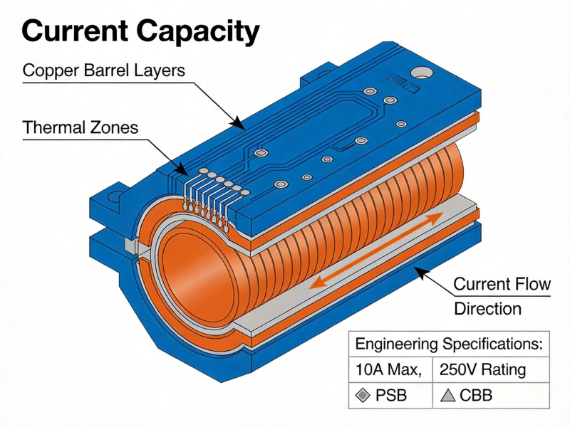
Plated Through Hole Current Rating: Complete Guide for PCB DesignersMay/21/2026
High Current PCB Design for Electric Vehicle Charging StationsAugust/15/2026
A Deep Dive into High Current PCB Design for Solar InvertersJuly/17/2026
High Current PCB Design for Audio Amplifiers: Avoiding Ground LoopsSeptember/14/2026
High Current PCB Pad Design: Reinforced Plating vs. Standard PadsJuly/28/2026
2oz vs. 4oz Copper: Which is Best for Your High Current PCB?July/10/2026
High Current PCB Design for Aerospace Power DistributionSeptember/08/2026
High Current PCB Design for Telecommunications Base StationsSeptember/18/2026