

Telecommunications base stations are among the most demanding environments for printed circuit board design. A single macro cell site houses power amplifiers, radio transceivers, filters, and baseband processing units — all running simultaneously, all generating heat, and all relying on a PCB infrastructure that must carry tens and sometimes hundreds of amps without excessive voltage drop, overheating, or signal integrity degradation. Designing PCBs for this world is not a matter of scaling up a standard board — it requires a fundamentally different approach to copper distribution, Thermal Management, Layer Stackup, and material selection.
This guide covers the engineering principles, design practices, and manufacturing considerations that matter most when designing high-current PCBs for telecom infrastructure.
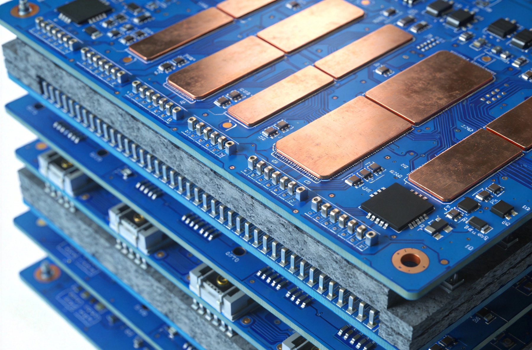
A typical LTE or 5G macro base station consumes between 500W and 3,000W of power, depending on the configuration and number of radio chains. The main power supply bus distributes 48V DC throughout the system, which is then converted down to lower rails — 12V, 5V, 3.3V, and sub-1V rails for digital ICs — through DC-DC converters mounted directly on the PCB.
At 48V, even a 1,000W load draws only about 21 amps. But after multiple conversion stages, the lower voltage rails can carry 50A, 100A, or more. A 1V rail supplying a power amplifier or FPGA core at 100A represents 100W of power in an area that might be no larger than a few square centimeters. This concentration of Current Density is the central challenge of high-current base station Pcb Design.
The consequences of getting the design wrong are severe: voltage droop under load peaks causes digital logic errors, excessive heat degrades component reliability and shortens service life, and electromigration — the gradual movement of copper atoms under High Current — can cause trace voids and eventual open circuits in the field.
Current-carrying capacity is primarily a function of trace cross-sectional area, Copper Weight, and temperature rise. The Ipc-2221 generic standard provides baseline current-carrying formulas, but for high-current telecom applications, the numbers in the standard are often insufficiently conservative.
Standard PCB Fabrication offers copper weights of 0.5oz, 1oz, 1.5oz, 2oz, 3oz, and heavier. For high-current traces in base station designs, 2oz and 3oz copper are common choices; for the most demanding power bus bars, 4oz to 6oz copper or even busbars bonded to the PCB surface may be required.
For a 50A continuous current on an external layer in a 10°C temperature rise scenario, Ipc-2221 suggests approximately 250 mil (6.35mm) of trace width with 2oz copper. That is a very wide trace — often impractical on a densely packed base station board. The solution in practice is to use wider traces on internal planes, distribute the current across multiple parallel traces, or move to heavier copper weights.
A practical design approach for high-current buses:
The Layer Stackup is the single most important design decision for a high-current base station PCB. A well-designed stackup provides low-resistance Power Distribution, effective thermal conduction away from heat sources, controlled impedance for RF signal traces, and adequate ground reference for signal integrity.
A typical high-current 8-layer base station board might use a stackup like this:
The key principle is to place Heavy Copper Power Planes adjacent to ground planes to maximize capacitance between adjacent layers and to use dedicated high-current planes with no segmentation — a solid uninterrupted plane carries more current than the same copper area split across multiple segments with gaps.
Heat generation in high-current PCBs is proportional to I²R losses. A trace carrying 100A with a total resistance of 0.5 milliohm dissipates 5W — not trivially small when concentrated in a single component footprint. Managing this heat requires a multi-pronged approach.
Components that generate significant heat — power MOSFETs, voltage regulators, power amplifiers — almost universally use Thermal Pad or exposed pad packages (D2PAK, QFN, TQFN, LGA). Connecting these pads to internal copper planes through thermal via arrays is the primary heat removal mechanism.
A well-designed thermal via array under a power package should use vias of 0.3–0.5mm diameter on 0.8–1.2mm pitch. The vias should be plated to at least 1oz copper throughout their barrel wall, and they should be fully landed on the target internal plane. Solder mask tenting on the via barrel prevents Solder Wicking during reflow, which would reduce thermal contact.
Thermal simulation using tools like Ansys Icepack, Siemens NX Thermal, or Cadence Sigrity PowerSI can predict junction temperatures before the board is fabricated, allowing optimization of via count, pitch, and plane geometry before committing to manufacturing.
For the highest-power components, passive or active heatsinks are often required. The Pcb Design must accommodate Heatsink Mounting points, thermal interface material (TIM) thickness control, and mechanical fastening. Aluminum core PCBs or metal-backed substrates (IMS — Insulated Metal Substrate) are commonly used for base station power stages where conventional FR-4 cannot adequately dissipate heat.
IMS boards use a dielectric layer with high thermal conductivity (typically 1–5 W/mK) between a copper circuit layer and an aluminum base. They can move heat from surface components to the base plate with thermal resistances 5–10x lower than standard FR-4, making them ideal for RF power amplifier stages and high-current Dc-dc Converter sections.
Many base station power modules incorporate liquid cooling channels or forced-air heatsinks. The PCB must be designed to interface cleanly with these cooling structures — typically through machined thermal pedestals or direct-bonded copper (DBC) substrates that bolt or clamp to the cooling plate. The mechanical design must account for thermal expansion mismatches between the PCB, substrate, and cooling plate to avoid stress-induced solder joint failures over thermal cycles.
In high-current systems, the resistance of Power Distribution traces causes voltage drop under load. If the drop is too large, downstream converters and components receive insufficient voltage, leading to regulation errors, logic failures, or premature shutdown.
A complete voltage drop (Ir Drop) analysis should be performed during the design phase. The analysis calculates the resistance of every segment of the power distribution network from the source to each load, determines the voltage at each load under worst-case current conditions, and compares it against the load's minimum operating voltage specification.
For a 48V power bus distributing current to multiple DC-DC converters, the total allowable Ir Drop from source to load is typically limited to 2–3% of the nominal voltage (about 1V for a 48V system). This budget must be allocated across connectors, Pcb Traces, vias, and any intermediate distribution components.
Key practices for minimizing IR drop in base station power distribution:
Base station equipment operates across a wide temperature range, from sub-zero winter conditions to sustained high temperatures in outdoor enclosures exposed to direct sunlight. Material selection must account for long-term reliability under Thermal Cycling, moisture resistance, and CAF (Conductive Anodic Filament) resistance.
Standard FR-4 with Tg 130°C is adequate for many base station applications, but for boards with high thermal loads or extended high-temperature operation, high-Tg materials — Tg 150°C, Tg 170°C, or high-Tg polyimide — provide better resistance to delamination and thermal expansion mismatch. The thermal coefficient of expansion (TCE) also matters: materials with TCE closer to that of copper (approximately 17 ppm/°C) produce less stress on plated through-holes during thermal cycling.
For high-frequency RF sections of the base station board, traditional FR-4 introduces excessive dielectric loss at frequencies above 3GHz. Rogers RO4000 series, Taconic RF materials, and Panasonic Megtron 6 are commonly specified for these sections. These materials offer lower dissipation factor and more stable dielectric constant across frequency and temperature, at higher material and Manufacturing Cost.
Conductive Anodic Filament (CAF) failure occurs when moisture and voltage stress cause copper to migrate along the glass fiber bundles in the PCB laminate, creating a short between adjacent signals or planes. For high-reliability telecom applications, specifying CAF-resistant laminate — with tighter resin content control and specific weave styles designed to reduce wicking — is strongly recommended, particularly for boards that will be deployed outdoors in humid environments.
Designing a High-current Pcb on paper means nothing if the fabrication process cannot produce it reliably. Heavy copper boards (2oz and above) have specific manufacturing requirements that must be planned for during the design phase.
Heavy copper boards require longer etching time, which can cause over-etching of fine traces on the same panel. To avoid this, designs that mix heavy copper power distribution with fine-pitch signal traces should specify different copper weights on different layers — heavy copper for planes and power traces, standard copper (1oz) for signal layers — rather than using uniform Copper Weight across all layers. This minimizes the risk of undercutting fine signal traces during the etch process.
High-current vias must carry substantial current between layers. Standard PCB plating of 0.8–1.0 mil (20–25μm) of copper may be insufficient for high-reliability applications. Specify minimum 1.2–1.5 mil (30–38μm) plating for high-current vias, and verify plating continuity with cross-section analysis of production panels. PTH (Plated Through-hole) reliability testing per IPC-T-50 and IPC-6012 Class 3 should be specified for telecom-grade boards.
Heavy copper boards are more susceptible to bow and twist due to the differential thermal expansion of thick copper and laminate during lamination and reflow. For large-format base station boards, specify bow-and-twist tolerances of 0.5% or tighter and specify panel flatness requirements in your fabrication notes. A warped board can cause placement accuracy problems during assembly and stress on heavy components during thermal cycling.
For heavy copper boards, the surface finish must be compatible with the thick copper and provide reliable solderability. HASL (Hot Air Solder Leveling) can be uneven on heavy copper boards due to the large thermal mass of thick copper features. ENIG (Electroless Nickel Immersion Gold) provides a flat, uniform surface ideal for fine-pitch component assembly and is the preferred finish for telecom-grade boards. For the highest reliability, consider gold thickness of 2–3μ" (micro-inches) over 120–160μ" of nickel to ensure adequate wire-bondable and solderable surfaces over the board's operating life.
Modern base station PCBs are not purely power distribution boards — they combine high-current power stages with sensitive RF signal paths, high-speed digital interfaces (10Gbps SerDes for CPRI/eCPRI fronthaul), and control logic. The coexistence of High Current and sensitive signals requires careful design attention.
Electrically noisy power stages — switching converters, Class-D amplifiers — should be physically separated from sensitive RF and high-speed digital sections. Use dedicated ground slots and partition the ground plane to prevent switching noise coupling into signal paths. RF power amplifier sections should have their own isolated ground return, tied to the main ground at a single point to prevent Ground Loop currents.
High-current switching stages generate broadband noise that couples through shared power rails. Place bulk decoupling capacitors (10μF–100μF) as close as possible to the power input pins of switching regulators. Use a cascade of bypass capacitors — large bulk caps for low-frequency decoupling, MLCCs (0.1μF–10μF) for mid-frequency, and small RF capacitors (10pF–100pF) for high-frequency — to provide a low-impedance AC path to ground across the entire frequency spectrum of the switching noise.
Telecom equipment is subject to some of the most demanding reliability requirements of any electronics application. Base station PCBs are expected to operate continuously for 20+ years in outdoor environments with minimal maintenance.
Key standards and test requirements:
Specify these requirements clearly in your fabrication and assembly documentation. Chinese manufacturers with telecom experience are familiar with these standards and can build to them reliably, but clear documentation prevents misunderstandings and ensures consistent quality across production batches.
High-current Pcb design for telecommunications base stations sits at the intersection of Power Electronics, thermal engineering, RF signal integrity, and long-term reliability. The demands are exceptional — tens to hundreds of amps, wide temperature ranges, multi-decade service life, and coexistence with sensitive RF signals — but the engineering principles are well understood and the manufacturing capability exists to produce these boards reliably.
Success comes from treating the PCB as a thermal and power distribution system, not just an interconnect substrate. Plan the layer stackup around current paths, verify thermal performance with simulation before fabrication, specify materials that match the environmental demands, and communicate all requirements — electrical, thermal, and reliability — clearly to your manufacturing partner. Boards designed with this level of rigor are the ones that keep base stations running reliably for 20 years in remote towers across every climate on earth.
For a continuous 100A bus, use at minimum 3oz copper on an internal plane layer, ideally 4oz or heavier for added margin. Route the bus as a solid uninterrupted plane rather than segmented traces, and use thermal via arrays (0.3–0.4mm vias on 0.8–1.0mm pitch) to connect surface components to the plane. Always run a voltage drop analysis to confirm that IR drop stays within 2–3% of the nominal voltage across the full current path.
Thermal Management for high-current PCBs requires a layered approach: use thermal via arrays under all major heat-generating packages, specify high-Tg or metal-core substrates for the most demanding power stages, place bulk decoupling and thermal interface materials strategically, and use thermal simulation tools to predict junction temperatures before fabrication. For the highest-power stages in 5G base stations, consider IMS substrates with thermal conductivity ratings of 1–5 W/mK in the dielectric layer.
Standard FR-4 has a glass transition temperature (Tg) of approximately 130°C. High-Tg FR-4 materials (Tg 150°C, 170°C, or higher) maintain their mechanical rigidity at higher temperatures, reducing the risk of delamination during multiple reflow cycles and under sustained high-temperature operation. For base station boards that operate in outdoor enclosures with significant self-heating, high-Tg materials provide a larger safety margin against thermal degradation over a 20-year service life.
Heavy copper boards (3oz and above) typically cost 20–40% more than standard 1oz boards due to longer etch times, thicker plating requirements, and tighter process control. Lead times are also slightly longer — typically 2–4 weeks versus 1–2 weeks for standard boards. However, the cost premium is justified when you consider that a field failure in a base station thousands of miles away costs far more than the PCB premium. Specify heavy copper clearly in your fabrication notes, including minimum copper weight, plating thickness requirements, and any panel flatness tolerances.
At high currents, even milliohm-level resistance in the power distribution network causes significant voltage drop. A total resistance of 20 milliohms at 100A results in a 2V drop — which could push a 5V rail down to 3V, causing downstream ICs to malfunction or shut down. Voltage drop analysis identifies every resistive element in the power path (traces, planes, vias, connectors, solder joints) and confirms that the voltage at each load remains within its specified operating range under worst-case current and temperature conditions.
ENIG (Electroless Nickel Immersion Gold) is the preferred surface finish for telecom-grade boards with high-current and fine-pitch mixed designs. It provides a flat, uniform surface that ensures reliable solder joints for both heavy components and fine-pitch BGA or QFN packages. For high-reliability applications, specify 2–3μ" of gold over 120–160μ" of nickel to ensure the finish maintains solderability and contact reliability over the full expected service life of the equipment.
High Current PCB Current Sensing: Shunt Resistor vs. Hall Effect LayoutJuly/29/2026
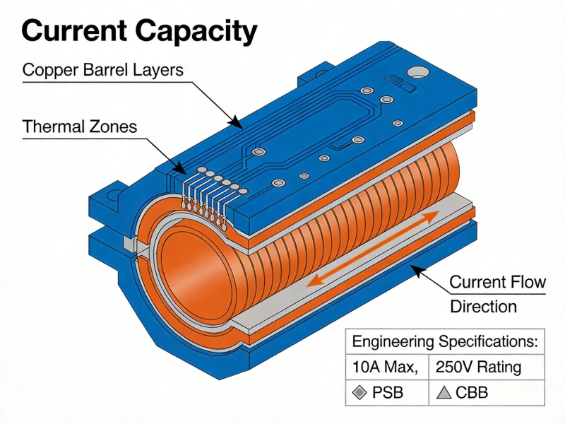
Plated Through Hole Current Rating: Complete Guide for PCB DesignersMay/21/2026
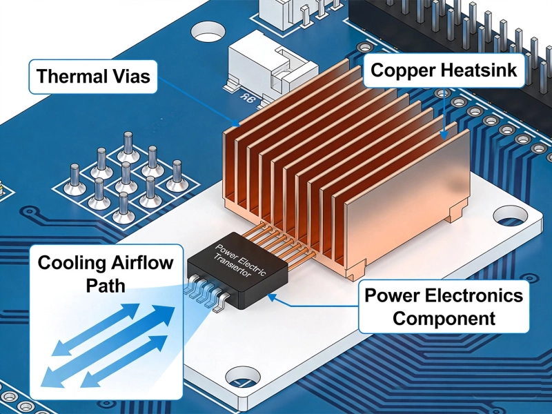
Why Your High-Power PCBs Overheat (And the 5 Methods That Actually Fix It)May/20/2026

High Current PCB Design for Railway Traction SystemsAugust/07/2026
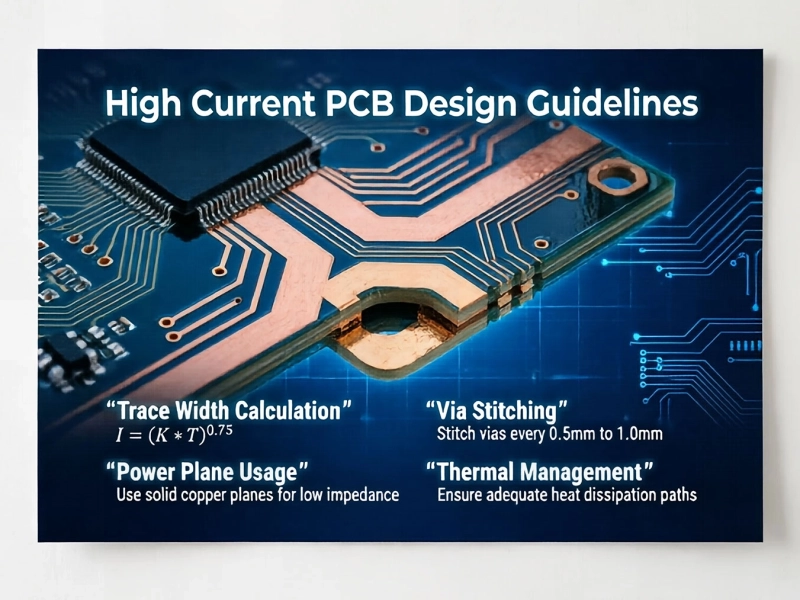
High Current PCB Design Guidelines: Ensuring Reliability and SafetyJune/08/2026
High Current PCB Design for Medical Imaging EquipmentSeptember/10/2026
Designing a 100A High Current PCB for EV Battery Management SystemsJuly/09/2026
5 Critical Thermal Management Problems in High Power PCBsMay/21/2026