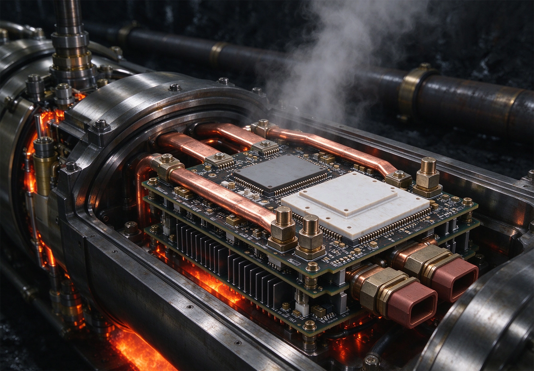
Downhole tools used in oil, gas, and geothermal drilling operations operate in some of the harshest environments on Earth. These tools are exposed to extreme temperatures ranging from 125°C to 225°C, high pressure up to 30,000 psi, constant vibration and shock, and must deliver reliable performance for months or even years without maintenance. For downhole tools that handle High Current loads, such as motor drivers, power supplies, and heating elements, Pcb Design is a critical factor that directly determines tool reliability and lifespan. A poorly designed High Current PCB can fail prematurely in downhole conditions, leading to costly downtime, lost production, and expensive tool recovery operations.

Unique Challenges of Downhole Environments for High Current PCBs
Designing High Current PCBs for downhole tools requires addressing a unique set of environmental challenges that do not exist in standard commercial or industrial applications:
- Extreme High Temperatures: Downhole temperatures can reach 225°C (437°F) or higher in deep wells, far exceeding the operating limits of standard FR4 PCB materials. High temperatures reduce the Current Carrying Capacity of copper traces, accelerate insulation degradation, and increase the risk of thermal fatigue failure.
- High Current Loads: Many downhole tools require high current to power motors, sensors, heating elements, and communication systems. These high currents generate significant additional heat on the PCB, compounding the effects of high ambient downhole temperatures.
- Pressure and Vibration: Downhole tools are exposed to extreme pressure and constant vibration during drilling operations. This mechanical stress can cause solder joint failures, PCB delamination, and component damage, especially in high current designs with Heavy Copper layers and large components.
- Long Service Life Requirements: Downhole tools are often deployed for months or years without access for maintenance or repair. PCB designs must deliver reliable performance over extended lifespans in extreme conditions, with zero tolerance for premature failure.
- Limited Space: Downhole tools have strict size constraints, requiring high current PCBs to fit into small form factors while still delivering high power and Heat Dissipation capabilities.
Critical Design Challenges for High Current Downhole PCBs
Designing high current PCBs for high-temperature downhole environments requires addressing several unique design challenges:
1. Reduced Current Carrying Capacity at High Temperatures
The Current Carrying Capacity of copper traces decreases significantly as temperature increases. At 200°C, a Copper Trace can only carry approximately 60% of the current it can carry at 25°C. This means standard current capacity calculations for room temperature operation are not sufficient for downhole applications, and designers must derate current carrying capabilities significantly for high temperature operation.
2. Thermal Expansion Mismatch
Different materials used in PCB construction have different coefficients of thermal expansion (CTE). In high temperature environments, this mismatch causes stress between copper traces, substrate materials, and component leads, leading to solder joint cracks, trace delamination, and PCB warping. This problem is amplified in high current designs that use thick copper layers, which have higher CTE than standard PCB substrates.
3. Insulation Material Degradation
Standard FR4 PCB substrates begin to degrade at temperatures above 125°C, losing insulation resistance and mechanical strength. In high current designs, the combination of high ambient temperatures and heat generated by current flow can accelerate this degradation, leading to electrical short circuits and PCB failure.
4. Heat Dissipation Limitations
Downhole tools are typically enclosed in sealed metal housings, with limited airflow for Heat Dissipation. All heat generated by high current circuits must be conducted through the PCB and tool housing to the surrounding wellbore fluid. Poor Thermal Design can lead to excessive component and PCB temperatures, even if the ambient downhole temperature is within design limits.
Best Practices for High Current Downhole PCB Design
Follow these design best practices to ensure reliable performance of high current PCBs in high-temperature downhole environments:
1. Select Appropriate PCB Materials
Material selection is the most critical factor in high-temperature downhole Pcb Design:
- Substrate Material: Use high-temperature, high-Tg (glass transition temperature) substrate materials specifically designed for extreme environments. Preferred materials include polyimide substrates with Tg above 250°C, or Ceramic Substrates for the highest temperature applications. Avoid standard FR4 materials, which are not suitable for temperatures above 125°C.
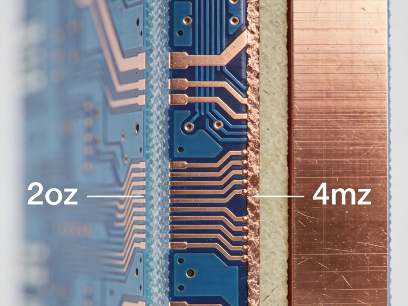
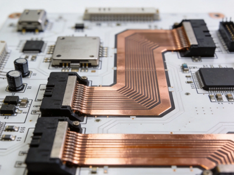
- Copper Foil Thickness: Use thick copper foil (2 oz to 10 oz) for high current paths to reduce resistance and increase current carrying capacity. Thick copper also improves heat dissipation and mechanical stability at high temperatures.
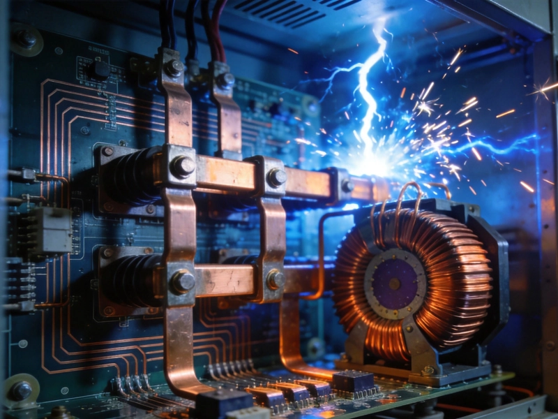
- Solder Mask and Insulation: Use high-temperature solder mask materials rated for continuous operation at 200°C or higher. For high-voltage high-current designs, use additional insulation layers between high current traces to prevent arcing at high temperatures.
2. Optimize Routing for High Current Operation
Proper routing is essential for reliable high current operation in high temperatures:
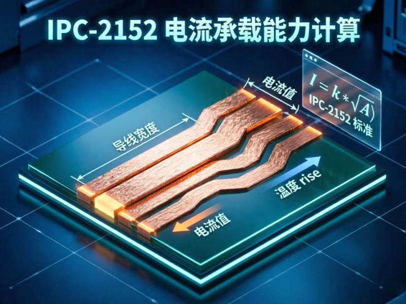
- Trace Width Calculation: Calculate trace width using high-temperature derating factors. As a general rule, derate current carrying capacity by 50% for operation at 200°C compared to room temperature ratings. Use wider traces than you would for standard industrial applications to reduce resistive heating and voltage drop.
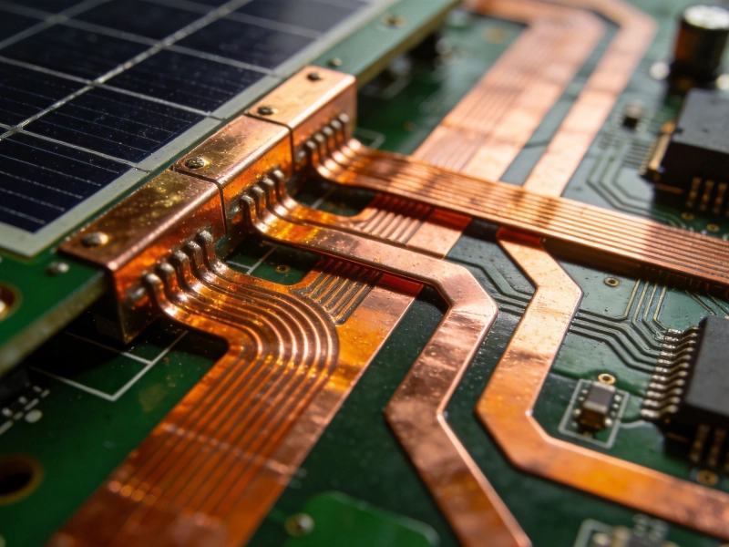
- Parallel Current Paths: For very high current applications, use multiple parallel traces on multiple layers to distribute current and reduce resistance. Ensure symmetric routing to ensure even Current Distribution across parallel paths.
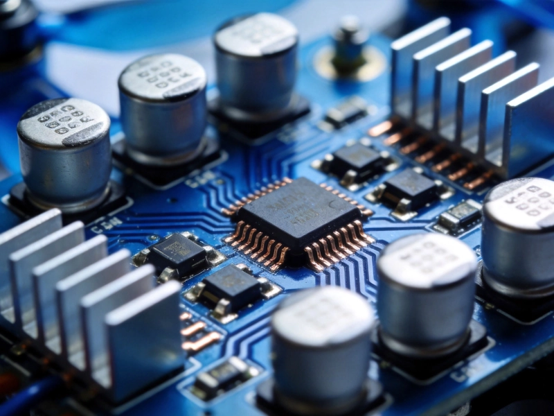
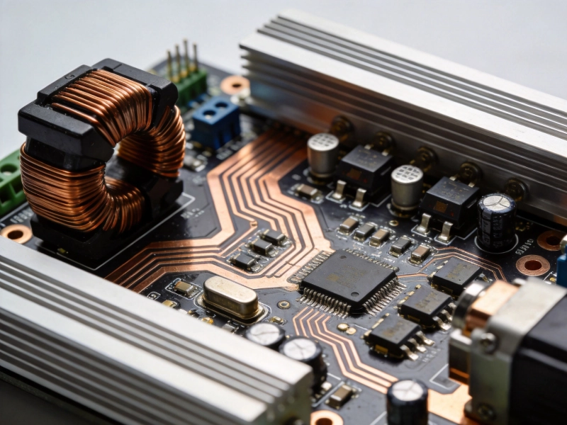
- Thermal Vias: Place large numbers of Thermal Vias under high-power components and high current traces to conduct heat away from the surface of the board to inner layers or the back of the PCB, where it can be dissipated through the tool housing.
- Avoid Sharp Corners: Use rounded corners and 45-degree angles on high current traces to avoid Current Crowding and hotspots at sharp corners.
3. Optimize Component Placement and Layout
Strategic Component Placement improves reliability and thermal performance:
- Distribute High-Power Components: Spread high-power components across the PCB to avoid creating concentrated hotspots. Place heat-generating components near the edge of the board or near mounting points that conduct heat to the tool housing.
- Short Current Paths: Minimize the length of high current paths to reduce resistance and resistive heating. Place power components close to each other and to input/output connectors to minimize trace length.
- Thermal Isolation: Isolate heat-sensitive components from high-power components and high current traces. Use thermal barriers or separate PCB sections for sensitive low-power circuits and high-power circuits.
- Vibration Resistance: Mount large, heavy power components using additional mechanical support, such as mounting brackets or adhesive, to prevent damage from vibration. Avoid placing heavy components near the edges of the board where vibration stress is highest.
4. Implement Reliability Enhancement Features
Add these design features to improve long-term reliability in extreme conditions:
- Redundant Current Paths: Add redundant traces for critical high current paths to provide backup in case of trace failure due to thermal fatigue.
- Wide Solder Pads: Use larger than standard solder pads for high current components to improve Solder Joint Reliability and reduce resistance at connection points.
- Impedance Control: Control impedance on high current paths to minimize voltage drop and ensure consistent performance across temperature ranges.
- Test Points: Include test points for current, voltage, and temperature monitoring to allow testing and validation of the PCB before deployment.
Testing and Validation Requirements
All high current downhole PCBs must undergo rigorous testing to validate performance in extreme conditions:
- High-Temperature Aging Test: Test the PCB under full current load at maximum operating temperature for 1000+ hours to validate long-term reliability.
- Thermal Cycling Test: Subject the PCB to repeated temperature cycles from -40°C to maximum operating temperature to validate resistance to thermal fatigue and CTE mismatch stress.
- Vibration and Shock Test: Test the PCB under vibration and shock conditions simulating downhole drilling environments to ensure mechanical reliability.
- Current Carrying Test: Verify that high current traces can carry rated current at maximum temperature without excessive temperature rise or trace failure.
- Insulation Resistance Test: Test insulation resistance at high temperature to ensure no breakdown or leakage between high current paths.
Conclusion
Designing high current PCBs for high-temperature downhole tools is a complex engineering challenge that requires careful consideration of material selection, routing, layout, and reliability enhancement features. The extreme environmental conditions of downhole operation leave no room for design errors, as even minor issues can lead to catastrophic tool failure and costly operational downtime. By following proven design best practices, selecting appropriate high-temperature materials, and conducting rigorous testing and validation, you can create High Current PCB designs that deliver reliable performance in even the harshest downhole environments.
Whether you're designing PCBs for logging tools, drilling motors, measurement while drilling (MWD) systems, or geothermal downhole tools, applying these design principles will help you achieve the long-term reliability required for downhole applications.
Contact us to discuss your requirements.
Frequently Asked Questions
Q: What is the maximum temperature rating for downhole PCBs?
A: Downhole PCBs are typically designed for continuous operation at temperatures between 125°C and 225°C, with some specialized designs capable of operating at temperatures up to 250°C or higher.
Q: What materials are best for high-temperature downhole PCBs?
A: Polyimide substrates with high Tg values (above 250°C) are the most common choice for downhole PCBs. For extremely high temperature applications, Ceramic Substrates may be used.
Q: How thick should copper layers be for high current downhole PCBs?
A: High current downhole PCBs typically use 2 oz to 10 oz thick copper layers, depending on the current requirements. Thicker copper provides higher current carrying capacity and better heat dissipation.
Q: How do I calculate trace width for high temperature downhole operation?
A: Calculate trace width using standard Ipc-2152 guidelines, then apply a derating factor of 50% for operation at 200°C to account for reduced current carrying capacity at high temperatures.
Q: What testing is required for downhole high current PCBs?
A: Required testing includes high-temperature aging, Thermal Cycling, vibration and shock testing, current carrying capacity testing, and insulation resistance testing at maximum operating temperature.