

Power Electronics demand printed circuit boards that can handle currents far beyond what standard PCB designs encounter. Whether you are building motor controllers for electric vehicles, inverters for solar installations, or welding equipment controllers, the PCB must reliably conduct and dissipate significant electrical power without degradation. Heavy Copper PCBs — boards with trace copper weights of 3 ounces per square foot or more — present unique manufacturing challenges, and few decisions more significantly impact manufacturability and reliability than the choice of solder mask application method.
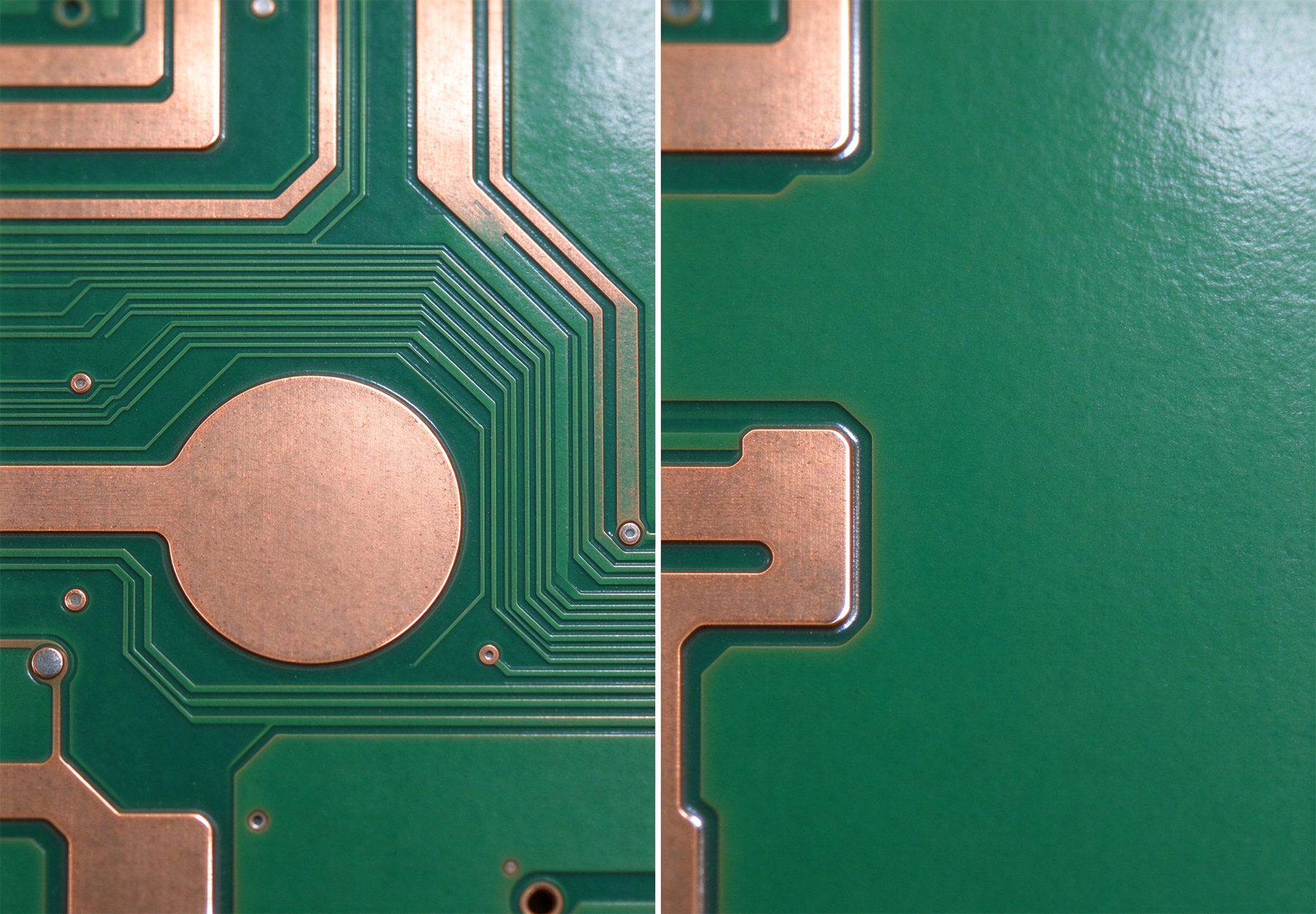
Solder mask serves multiple purposes on any PCB, but its role becomes particularly critical in Heavy Copper applications. The primary function remains the same: solder mask prevents unintended solder bridging during assembly and protects the copper surface from oxidation and environmental contamination. In High Current designs, however, solder mask also influences thermal performance and the board's ability to operate at elevated temperatures without degradation.
Standard PCB solder masks are thermosetting polymers that cure to a hard, chemically resistant finish. The typical cured thickness ranges from 0.5 mils to 1.5 mils across the board surface. For standard digital logic circuits operating at low currents, this thickness is entirely adequate. For heavy copper designs conducting 20, 50, or 100+ amps, the cumulative Thermal Resistance of thin solder mask layers across large unvented areas can meaningfully impact the board's thermal performance.
Understanding how different solder mask application methods affect coverage uniformity, cured thickness, and conformance to irregular board topographies enables engineers to make informed decisions that balance manufacturability, cost, and performance.
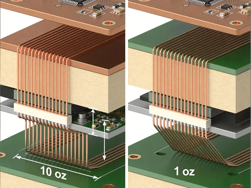
Heavy copper PCBs are defined by their use of extended copper weights — typically 3 oz/ft² (105 μm) or greater, compared to the 1 oz/ft² (35 μm) standard for most consumer electronics. Some Power Electronics applications push this further, utilizing 6 oz/ft², 10 oz/ft², or even thicker copper plating for Bus Bar applications where current handling exceeding 500 amps may be required.
The manufacturing processes for heavy copper boards diverge from standard PCB production in several important ways. Etching thick copper requires extended processing time and different chemical concentrations. Drill parameters must account for increased tool wear. Via plating requires longer electroplating cycles to achieve adequate Copper Thickness in the barrel. And solder mask application must accommodate the pronounced topographic variations that heavy copper circuitry creates on the board surface.
This topography is the crux of the solder mask challenge. A 5-ounce Copper Trace standing 175 micrometers proud of the surrounding base material creates significant elevation changes across the board. Standard solder mask application processes designed for flat surfaces may struggle to coat the vertical walls of heavy copper features uniformly, potentially leaving thin spots or voids where contamination and oxidation can take hold.
Dam application, also called selective solder mask application or mask dam printing, deposits solder mask material only where coverage is required, leaving heavy copper bus bars and current-carrying traces exposed or minimally coated. This approach treats the solder mask as a precisely applied barrier rather than a blanket coating across the entire board surface.
The dam application process uses screen printing or pneumatic dispensing equipment to deposit precise amounts of liquid solder mask material along defined boundaries. The mask material is typically a two-part epoxy or acrylic formulation with thixotropic properties that enable it to hold a defined bead height without slumping. After application, the mask cures through thermal or UV exposure, creating raised barriers that effectively contain solder during assembly operations.
The resulting structure resembles a miniature dam wall built up along the perimeter of components and connector areas. This built-up edge provides excellent solder containment even when the underlying copper surface is not fully coated. For boards with large exposed copper areas intended for high-current conduction, dam application naturally leaves these areas uncoated, which is often the desired outcome for thermal and electrical reasons.
The primary advantage of dam application is coverage control. By selectively applying mask only to areas that require protection, manufacturers eliminate the risk of voids or thin spots over irregular heavy copper topographies. The mask that is applied achieves adequate thickness because it is not spread thin across large uneven areas.
Thermal performance benefits emerge because exposed heavy copper surfaces can interface directly with thermal pads, Heat Sinks, or forced-air cooling without the Thermal Resistance penalty of intervening solder mask layers. In High Current applications where junction temperatures directly impact reliability, this improved thermal path can meaningfully extend component lifetime.
Material cost savings also favor dam application for boards with extensive exposed copper areas. Covering 60 percent of the board surface with solder mask costs more than covering 30 percent, and the economics improve further when the mask that is applied achieves better coverage with fewer defects requiring rework.
Dam application requires more complex tooling and process control than flood application. The screen or stencil used for mask deposition must be manufactured to tighter tolerances, and the application equipment must maintain consistent dispensing pressure and speed. Setup time and tooling costs increase accordingly, making dam application less economical for very simple board layouts with minimal heavy copper features.
Edge definition and consistency require careful process control. Inconsistent dam height or width can compromise solder containment, leading to bridging defects during assembly. Boards with very high component density may not provide adequate space between components to accommodate dam walls, limiting the applicability of this approach.
Flood application, also called curtain coating or spray coating, applies solder mask as a continuous layer across the entire board surface, following the contours of underlying features. This method accommodates irregular topographies without requiring precise placement of material boundaries.
Flood application methods include curtain coating, where liquid solder mask flows over the board surface in a continuous thin film, and spray application, where atomized mask material is applied in controlled passes. Vacuum impregnation may follow, drawing mask material into small voids and ensuring complete coverage around feature edges. The result is a conformal coating that follows the topography of heavy copper features rather than building up along defined boundaries.
The process handles irregular board surfaces naturally because the coating material flows into recesses and around features. Heavy copper traces receive solder mask on their vertical walls as well as their horizontal surfaces, providing complete environmental protection across all exposed copper areas. This comprehensive coverage eliminates the risk of oxidation or contamination on any portion of the exposed copper network.
Flood application provides superior conformal coverage over irregular topographies. Heavy copper features with significant height variation receive consistent coating because the application method adapts to the surface profile rather than requiring material to be placed at specific locations. This characteristic makes flood application the default choice for boards with complex routing and varied copper weights.
Process simplicity favors flood application for many board configurations. Without the need for precise selective deposition, equipment setup is more straightforward and process control requirements are less demanding. This simplicity translates to more predictable manufacturing costs and faster production cycles, particularly for boards without extensive exposed copper areas.
Environmental protection is more comprehensive with flood application. Every exposed copper surface, including the vertical walls of heavy copper traces and the small features between large conductors, receives coating. This uniform protection minimizes the risk of localized corrosion or contamination that could eventually compromise reliability.
The primary limitation of flood application on heavy copper boards is inadequate coverage in areas with large height variations. When thick solder mask is applied across an irregular surface and then cured, the coating may be thinner on vertical walls and at the edges of features where surface tension pulls the liquid mask away. These thin areas can be vulnerable to cracking during Thermal Cycling or to pinhole defects that compromise long-term protection.
Thermal performance suffers because every exposed copper surface is covered with a polymer layer. For high current designs where maximum copper-to-heat-sink contact is desired, this blanket coverage requires thermal interface materials to bridge the solder mask layer, adding thermal resistance to the Heat Dissipation path.
The decision between dam and flood application depends on several factors specific to each design and production scenario. Understanding these tradeoffs enables engineers to specify the appropriate approach rather than leaving the choice to default manufacturing processes.
Boards with mild Copper Weight variations — 3 oz/ft² copper on primarily 1 oz/ft² base — typically accommodate flood application without significant coverage concerns. The topographic variations are modest enough that conformal coating achieves adequate thickness even in challenging areas. For these boards, the process simplicity and comprehensive protection of flood application generally outweigh the thermal performance advantages of dam application.
Boards with extreme Copper Weight variations — 10 oz/ft² bus bars transitioning to 1 oz/ft² signal traces, for example — present more challenging coverage requirements. The heavy copper features stand significantly above the surrounding surface, and flood application may struggle to achieve adequate coverage on the vertical surfaces. Dam application or a hybrid approach becomes more attractive for these designs.
Designs with aggressive Thermal Management requirements — where the PCB must interface directly with Heat Sinks or thermal planes — favor dam application. Exposed copper surfaces can achieve metal-to-metal contact with thermal interface materials without intervening solder mask layers. For power electronics where component junction temperatures approach design limits, this thermal improvement can significantly extend operational lifetime.
Designs with less demanding thermal requirements may accept the thermal penalty of flood-applied solder mask. If component junction temperatures are well within ratings even with conformal mask coverage, the superior environmental protection of flood application may be the deciding factor.
Prototype and low-volume production runs often favor flood application for simplicity and faster turnaround. The additional tooling cost and process complexity of dam application are harder to justify when producing small quantities, and the per-board Manufacturing Cost for flood application is typically lower.
Medium and high-volume production of heavy copper boards frequently justifies the investment in dam application tooling. The per-unit cost savings from reduced mask material consumption and improved first-pass yield offset the tooling amortization over production runs of hundreds to thousands of boards. For products with long production lifecycles, the economics consistently favor optimized dam application processes.
In practice, many Heavy Copper Pcb manufacturers offer hybrid approaches that combine elements of both methods. A common hybrid approach applies flood coating across the board for baseline coverage, then follows with selective dam application around high-vulnerability areas or for enhanced solder containment. This combination captures advantages of both methods at the cost of increased process complexity.
Process optimization for heavy copper solder mask extends beyond the choice between dam and flood. Pre-treatment of the board surface, including chemical cleaning and micro-etching, improves solder mask adhesion to copper surfaces. Proper cure profile development — including adequate ramp rates and soak times — ensures complete crosslinking throughout the mask thickness. Post-cure inspection using automated optical systems identifies coverage defects before they propagate into assembly failures.
For the most demanding applications, some manufacturers specify multiple thin flood coat applications rather than a single thick application. Building up coverage in multiple passes reduces the risk of voids and achieves more uniform thickness across irregular topographies. While this approach increases process time, the improved coverage reliability justifies the additional cycle time for mission-critical power electronics.
Verifying solder mask coverage on heavy copper boards requires inspection methods that can detect thin spots, voids, and adhesion failures. Visual inspection under magnification provides gross defect detection but cannot reliably identify thin areas or micro-voids that may compromise long-term reliability. More comprehensive inspection methods include:
Cross-sectional analysis through microsectioning reveals actual coating thickness and adhesion characteristics at specific board locations. While destructive, this method provides definitive data on coverage uniformity that no non-destructive technique can match. For qualification testing of new board designs or process changes, microsectioning is the gold standard for solder mask evaluation.
Insulation resistance testing measures the electrical resistance between adjacent copper features after solder mask application. Low resistance readings indicate potential mask defects or contamination that could lead to leakage currents or short circuits under field conditions. This electrical test complements visual inspection by detecting functional defects that may not be visible.
Thermal shock testing subjects boards to rapid temperature cycling to identify solder mask defects that may not manifest under normal operating conditions. Cracking, delamination, or adhesion failures triggered by thermal stress reveal vulnerabilities that could cause field failures. For power electronics expected to operate in demanding environments, thermal shock testing provides essential qualification data.
What copper weight is considered heavy copper for PCB applications?
Heavy copper typically refers to copper weights of 3 oz/ft² (105 μm) or greater. Extended heavy copper includes weights from 6 oz/ft² up to 20 oz/ft² or more, used in Bus Bar applications and very high current Power Distribution.
Can heavy copper boards use standard solder mask formulations?
Standard solder mask formulations work for heavy copper applications, but the specific formulation may need adjustment for improved flow characteristics or thixotropic properties that accommodate irregular topographies. Discuss formulation requirements with your manufacturer early in the design process.
Does exposed copper require any surface treatment?
Exposed copper surfaces intended for high-current conduction or thermal interfacing typically receive Hasl (hot air solder leveling), Enig (electroless nickel gold), or OSP (organic solderability preservative) finishes to prevent oxidation and maintain solderability where future assembly or rework may be required.
What is the typical solder mask thickness for heavy copper boards?
Cured solder mask thickness on heavy copper boards typically ranges from 0.8 mils to 2.0 mils depending on application method and board topography. Coverage uniformity is more important than maximum thickness.
How do I determine whether dam or flood application is right for my design?
Consider your board topography complexity, Thermal Management requirements, production volume, and environmental protection needs. For designs with extreme copper weight variations and aggressive thermal requirements, dam application offers clear advantages. For simpler topologies with comprehensive environmental protection needs, flood application may be more appropriate. Discuss your specific requirements with your PCB manufacturer early in the design cycle.
Contact us to discuss your requirements.
High Current PCB Connector Selection Guide: Choosing the Right Power Connectors for Your Electronics ProjectsJune/12/2026

High Current PCB Testing: Thermal Imaging vs. 4-Wire Kelvin MeasurementJuly/22/2026
High Current PCB Heat Sinks: Thermal Pads vs. Direct Copper ExposureAugust/10/2026
High Current PCB Design for Telecommunications Base StationsSeptember/18/2026
Heavy Copper vs Standard Copper PCB: Complete Comparison Guide for EngineersMay/20/2026
High Current PCB Component Placement: Grouping vs. Distributed LayoutJuly/21/2026
High Current PCB Design for Electric Forklifts: A Practical Engineering GuideOctober/13/2026

A Deep Dive into High Current PCB Design for Solar InvertersJuly/17/2026