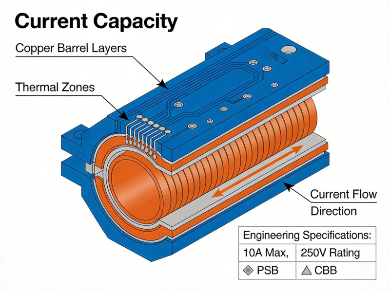
High-power RF amplifiers sit at the intersection of two demanding disciplines: high-current power delivery and high-frequency signal integrity. A 100-watt LDMOS amplifier at 2 GHz may draw 10 amperes of drain current while its output matching network must maintain 50-ohm impedance with sub-0.5 dB insertion loss. The PCB must handle both realities simultaneously—thick copper for current capacity and low inductance for RF performance—without letting one compromise the other. This article covers the design practices that make that possible.

The Dual Challenge: Current and Frequency
Standard Pcb Design Guidelines address either Power Distribution or RF signal routing—but rarely both at once. In a high-power RF amplifier, the two overlap in ways that create unique constraints:
- Current Density: Supply rails and drain feeds carry several to tens of amperes. Insufficient copper cross-section causes resistive heating, voltage droop under load, and eventual trace delamination or fusing.
- RF skin effect: At frequencies above 100 MHz, current crowds toward the conductor surface. The effective cross-section carrying RF current is far smaller than the physical trace thickness, which means a wide trace that handles DC current easily may still have excessive RF resistance.
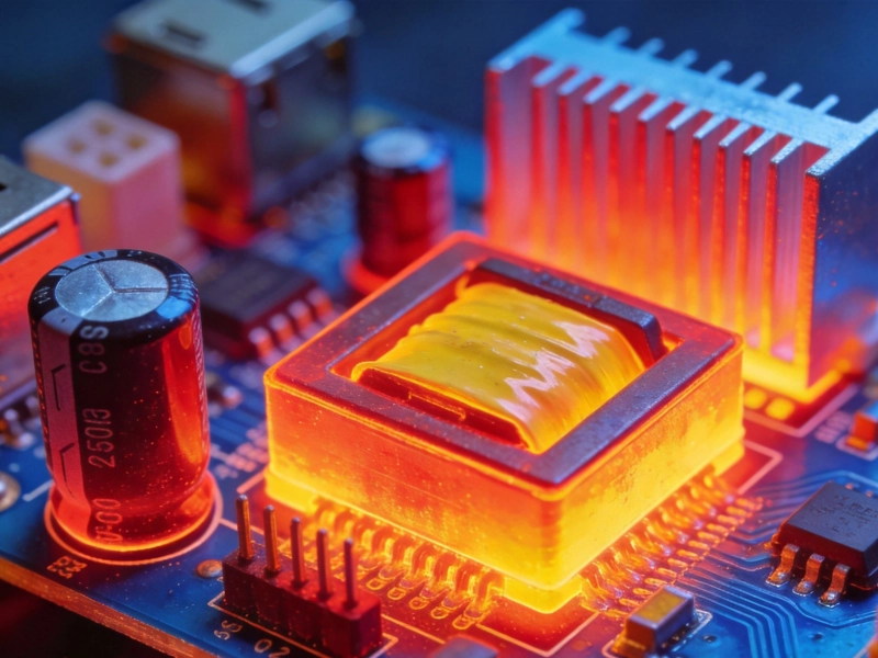
- Thermal Management: Power dissipation in the amplifier die and matching network resistors generates heat that must flow through the PCB to a heat sink. The PCB is not just an electrical interconnect—it is a thermal interface.
- Impedance control: Input and output matching networks require controlled-impedance transmission lines (microstrip, stripline, or coplanar waveguide). These structures are sensitive to Copper Thickness, substrate dielectric constant, and Trace Geometry—all of which are also influenced by current-carrying and thermal requirements.
Designing for all four simultaneously is the core challenge of high-current RF Pcb Design.
Copper Weight Selection for RF Power Amplifiers
Copper Weight (thickness) is the single most impactful material choice in RF amplifier Pcb Design. It affects current capacity, thermal conductivity, RF loss, and impedance—often in conflicting directions.
Standard Copper Weights and Their Trade-Offs
- 1 oz (35 µm): Adequate for signal traces and low-power RF. Insufficient for drain supply rails carrying more than 2–3 A without very wide traces. Lowest RF insertion loss for narrow impedance-controlled lines because the skin-depth penalty is minimal.
- 2 oz (70 µm): The most common choice for medium-power amplifiers (10–50 W). Doubles the DC current capacity and reduces trace resistance by half. Slightly increases RF loss in impedance-controlled microstrip because the wider trace (needed to hit the target impedance on thicker copper) has more surface area for skin-effect losses.
- 3 oz (105 µm) and 4 oz (140 µm): Used for high-power amplifiers (50–300 W) where drain feeds carry 10–30 A. Excellent current capacity and thermal spreading, but impedance control becomes harder—thick copper requires very wide microstrip traces for 50-ohm impedance, which may not fit the layout. Many designers use Heavy Copper on power layers only, with 1 oz on RF signal layers.
Asymmetric Stack-Up Strategies
The most effective approach for high-power RF amplifiers is an asymmetric copper allocation:
- RF signal layers: 1 oz or 2 oz copper for impedance-controlled transmission lines and matching networks
- Power/ground layers: 3 oz or 4 oz copper for drain supply planes, thermal spreading, and ground return
- Inner signal layers: 1 oz for control signals, bias networks, and low-current logic
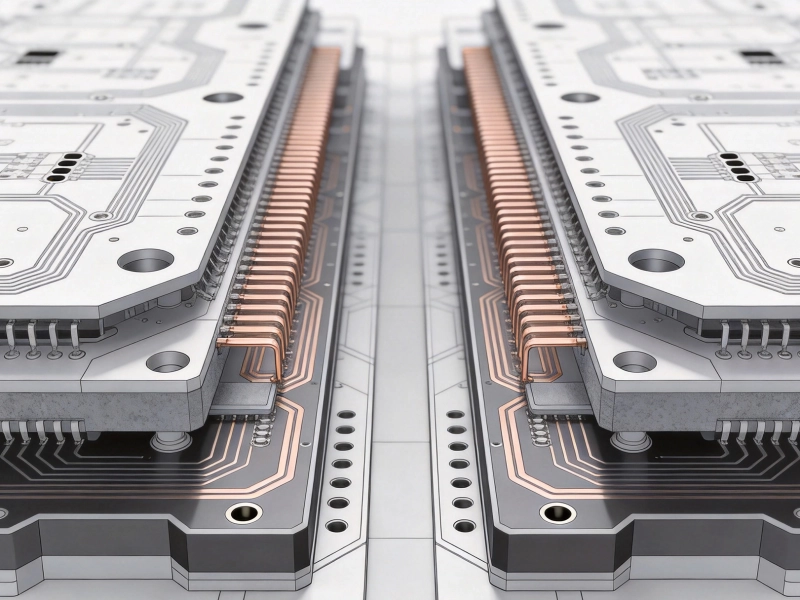
This hybrid approach lets you achieve 50-ohm impedance on RF traces without excessive width while still providing Heavy Copper for Power Distribution. Most PCB fabricators support mixed copper weights in a single stack-up, though cost increases with the number of different weights.
Current Capacity: Trace Width and Thermal Rise
The Ipc-2152 standard provides the authoritative method for sizing traces based on allowable temperature rise, current, and Copper Weight. For high-power RF amplifiers, the key considerations go beyond basic trace sizing:
Internal vs. External Traces
Internal traces (embedded in the substrate) have lower current capacity than external traces of the same cross-section because the substrate traps heat. A 4 oz internal trace may carry only 60–70% of the current of an equivalent external trace for the same temperature rise. For drain supply feeds, prefer external layers whenever possible.
Temperature Rise Budget
In RF amplifier designs, the PCB is already heated by the amplifier die and matching network losses. A trace temperature rise of 10 °C above ambient—conservative for general electronics—may be unrealistic when the board surface is already 40–60 °C above ambient from device dissipation. Design trace widths for the actual local ambient temperature, not the room ambient. A trace that can carry 10 A at 25 °C ambient with 10 °C rise may need to be 40–50% wider to carry the same current at 60 °C local ambient.
Via Current Capacity
Drain supply connections often transition between layers through vias. A standard via (0.3 mm finished hole, 1 oz plating) can carry approximately 0.5–1 A depending on temperature rise. For 10 A drain current, you need at least 10–20 vias in parallel. These vias should be placed in an array (via fence) around the device drain pad—not in a single row—to minimize inductance and distribute current evenly.
Thermal Management Strategies
Thermal Management in RF amplifier PCBs has two distinct paths: conduction through the board to a heat sink, and spreading laterally within the copper layers to reduce hot-spot intensity.
Thermal Vias Under the Amplifier Die
Most high-power RF transistors (LDMOS, GaN HEMT) are designed for bottom-side heat extraction through the device flange or bare die attach. The PCB must provide a low-thermal-resistance path from the device mounting pad to the heat sink:
- Via-in-pad thermal arrays: Place a grid of filled and capped vias directly under the device mounting pad. Typical density: 1 via per 1–2 mm². Via fill with copper (not solder) provides the highest thermal conductivity—approximately 400 W/m·K for copper vs. 50–60 W/m·K for solder fill.
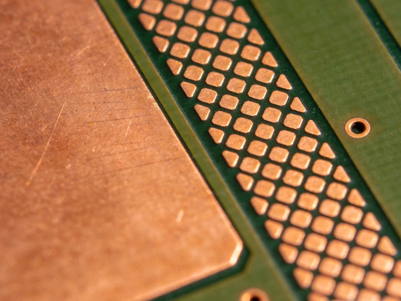
- Copper coin or embedded heat slug: For the highest-power designs (>100 W per device), a solid copper coin embedded in the PCB provides Thermal Resistance below 0.1 °C/W from die to heat sink. The coin replaces the FR-4 substrate locally and solders directly to the device flange on one side and the heat sink on the other.
- Direct attach to heat sink: Some designs cut a window in the PCB under the device so the transistor flange bolts directly to the heat sink, bypassing the PCB entirely. This is the lowest Thermal Resistance path but complicates Pcb Assembly and prevents routing traces through the device area.
Copper Pour Thermal Spreading
Large copper pours on inner ground layers act as lateral heat spreaders, distributing the heat from the device attachment area across a wider area of the board. This reduces the peak temperature at the device and lowers the thermal resistance to the heat sink by increasing the effective contact area.
For best results, avoid thermal reliefs on the ground plane pads of the amplifier device and its matching network components. Thermal reliefs are appropriate for low-power hand-soldered connections, but they add 2–5× thermal resistance at high-power device pads. A solid connection to the ground plane provides the lowest thermal path.
Impedance Matching Network Design on PCB
Input and output matching networks for RF power amplifiers are typically implemented as distributed (transmission line) or lumped-element structures on the PCB. Both approaches have current-handling implications.
Distributed Matching (Transmission Line Stubs and Transformers)
At frequencies above 1–2 GHz, distributed matching using microstrip or stripline elements is preferred:
- Line width vs. impedance: A 50-ohm microstrip line on 2 oz copper over a 0.5 mm substrate is approximately 0.9 mm wide. The same impedance on 4 oz copper requires a wider trace (~1.3 mm), which increases RF conductor loss because more copper surface area interacts with the skin-effect Current Distribution.
- Tapered lines: Impedance transformers implemented as tapered microstrip lines carry the full RF output current at their narrow end. Ensure the narrow section has sufficient copper cross-section for the peak current, which can be 2–3× the RMS value in Class AB or Class E amplifiers.
- Stub current handling: Open and shorted stubs carry standing-wave currents that can exceed the main line current at the stub tip. Size stub widths for the peak standing-wave current, not just the forward power.
Lumped-Element Matching (Capacitors and Inductors)
At lower frequencies (HF to low UHF), lumped-element matching is more compact:
- Blocking capacitors: Carry the full RF output current. Use high-Q, high-current capacitors (e.g., ATC 100B series, Murata GQM series) and connect them with wide, short traces to minimize series inductance. The trace from the device drain to the blocking capacitor should be as short as possible—every millimeter adds inductance that degrades the match at higher frequencies.
- Shunt capacitors: Carry a fraction of the RF current determined by the matching network topology. Size traces to shunt capacitors for the expected current, and place ground vias immediately adjacent to the capacitor ground pad to minimize ground path inductance.
- Inductors: Air-core or spring coils are common in HF/VHF matching networks. Their current capacity is determined by wire gauge, not Pcb Trace Width, but the PCB pads connecting to them must carry the same current. Use large pads with multiple connecting traces (spoke pattern) for high-current inductor connections.
Supply Decoupling and Bias Line Design
RF power amplifier bias lines (gate and drain supplies) must deliver high DC current without injecting noise or allowing RF energy to propagate back into the supply. This requires a decoupling strategy that addresses both low-frequency (power supply ripple) and high-frequency (RF signal) regimes.
Multi-Stage Decoupling
A robust decoupling network uses at least three capacitor values in parallel, each targeting a different frequency range:
- Bulk capacitors (10–100 µF, tantalum or aluminum): Placed closest to the supply entry point. Handle low-frequency droop during envelope transients (common in modulated signals).
- Medium capacitors (100 nF – 1 µF, X7R ceramic): Placed near the amplifier device. Decouple mid-band frequencies where supply impedance must be low.
- RF bypass capacitors (10–100 pF, NP0/C0G ceramic): Placed as close as physically possible to the device drain and gate pads. Provide a low-impedance path at the operating frequency, preventing RF from entering the supply rail.
Bias Line Chokes and Isolation
Between the decoupling network and the supply source, a choke (RFC) or quarter-wave line isolates the RF signal from the power supply:
- Conical chokes: Provide wideband isolation with high self-resonant frequency. Best for multi-octave or broadband amplifiers.
- Quarter-wave transmission line: At a single frequency, a λ/4 high-impedance line presents an open circuit at the amplifier end, providing excellent isolation with minimal loss. Widely used in narrowband VHF/UHF amplifiers.
- Ferrite bead chokes: Effective at lower frequencies (HF/VHF) but lossy at UHF and above. Select bead material for the impedance peak at your operating frequency.
The bias line trace itself must carry the full DC current and should be sized per Ipc-2152. However, unlike a pure DC supply trace, the bias line also carries superimposed RF current that the choke has not fully suppressed. Use wider traces than the DC calculation alone would require, and avoid narrow neckdowns near the device that create current bottlenecks.
Grounding Architecture for RF Amplifiers
Grounding is arguably the most critical aspect of RF amplifier PCB design. A poor ground structure creates common-impedance coupling between stages, promotes oscillation, and degrades output power and efficiency.
Continuous Ground Plane
Use an unbroken ground plane on the layer immediately below the RF signal layer. No cuts, no splits, no traces routed on the ground layer in the RF section. This plane provides:
- Low-inductance return path for RF signal currents (current returns directly beneath the signal trace at high frequency)
- Controlled impedance for microstrip transmission lines
- Thermal spreading from the device area
- Shielding between the RF section and control/logic circuitry
Ground Vias and Via Fencing
Ground vias connect the top-layer ground pours to the internal ground plane at regular intervals, preventing ground plane slot-line resonances and ensuring that the top-layer pour acts as a true RF ground:
- Via spacing: λ/20 or less at the highest operating frequency. At 2 GHz on FR-4, this means via spacing ≤ 7.5 mm. Closer spacing (λ/30 to λ/40) is better near the amplifier device and along the edges of RF Shielding Cans.
- Via fence along trace edges: A row of ground vias along the edges of microstrip lines and matching structures prevents fringing field coupling to adjacent circuits. This is especially important in push-pull and balanced amplifier topologies where two amplifier paths run in close proximity.
- Via fence at section boundaries: Where the RF section meets the control/bias section, a via fence (sometimes called a "ground wall") provides isolation, reducing feedthrough of RF energy into sensitive bias and control circuits.
Star Grounding for DC Returns
While RF grounds must be continuous and low-inductance, DC bias returns benefit from a star topology that prevents bias currents from one stage from flowing through ground conductors shared with another stage. In practice, this means:
- RF ground plane handles all RF return currents (continuous, unbroken)
- DC bias returns connect to the ground plane at a single point near the power supply entry
- Sequencing and protection circuitry grounds tie to the bias return point, not to the RF ground plane near the amplifier
Shielding and Isolation
High-power RF amplifiers generate strong electromagnetic fields that can couple into adjacent circuits, feedback paths, or even the input matching network—causing oscillation. Proper shielding is essential:
RF Shielding Cans
- Place Shielding Cans over each amplifier stage (driver, pre-driver, final) with via fences along the can footprint to ground the can to the ground plane at λ/20 intervals or less.
- Use partitioned cans (separate cavities for input and output matching) in high-gain designs to prevent cavity coupling between input and output.
- Design can dimensions to avoid cavity resonances at the operating frequency or its harmonics. A cavity resonance at the operating frequency can create positive feedback paths that cause oscillation.
Board-Level Isolation
- Route the input matching network on the opposite side of the amplifier device from the output matching network, with a ground via fence between them.
- Keep the RF path progression linear (input → device → output) without doubling back, which creates proximity coupling between high-power output and sensitive input.
- Separate control and bias circuitry from the RF section by at least 5–10 mm, with ground via fencing at the boundary.
Material Selection for RF Amplifier PCBs
The substrate material affects dielectric loss, thermal conductivity, and dimensional stability—all critical for RF amplifier performance:
FR-4 (Standard Epoxy Glass)
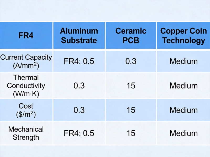
Adequate for HF/VHF amplifiers where dielectric loss is modest. Its thermal conductivity (~0.3 W/m·K) is poor, making it unsuitable for high-dissipation designs without significant thermal via infrastructure. Dissipation factor (tan δ) of ~0.02 at 1 GHz causes noticeable loss in output matching networks at UHF and above.
High-Frequency Laminates (Rogers RO4003C, RO4350B, RT/Duroid 6035HT)
Lower loss (tan δ = 0.002–0.004), better dimensional stability, and tighter dielectric constant tolerance. Essential for amplifiers operating above 1 GHz or where output matching network loss must be below 0.3 dB. Some high-frequency laminates have thermal conductivity of 0.6–0.8 W/m·K, a meaningful improvement over FR-4.
Hybrid Stack-Ups
Many RF amplifier designs use a hybrid stack-up: high-frequency laminate for the RF signal layer and ground plane, with FR-4 for inner control and power layers. This provides the RF performance of a low-loss laminate at a fraction of the cost of an all-low-loss stack-up. Bonding the dissimilar materials requires careful CTE matching to prevent delamination during Thermal Cycling.
Layout Review Checklist
Before releasing a high-power RF amplifier PCB for fabrication, verify these critical items:
- Drain supply trace widths meet IPC-2152 requirements at the maximum local ambient temperature
- Thermal via array under amplifier device is specified (quantity, fill material, diameter)
- Ground plane is unbroken in the RF section—no signal traces on the ground layer
- Via fences along all RF trace edges and at section boundaries, spacing ≤ λ/20
- Matching network traces maintain target impedance (verify with field solver, not simple calculators)
- Decoupling capacitors placed in descending value order, with smallest value closest to device
- No thermal reliefs on amplifier device ground pads
- Bias choke or quarter-wave isolator between supply and decoupling network
- Shielding can footprints include via fencing and avoid cavity resonances
- Copper weights specified per layer in the stack-up drawing (asymmetric allocation)
- Board edge plating specified if edge-launched RF connectors are used
Conclusion
High-current Pcb design for RF power amplifiers requires balancing electrical, thermal, and electromagnetic constraints that often pull in opposite directions. Heavy copper carries current but complicates impedance control. Thermal Vias remove heat but can disrupt ground plane continuity. Wide traces reduce DC resistance but increase RF conductor loss. The solutions lie in thoughtful stack-up design—placing heavy copper where it is needed for power and thermal management while keeping RF signal layers on thinner copper for impedance control—and in layout practices that respect both the current paths and the field distributions of a high-power RF circuit. By applying the techniques described here, from asymmetric copper allocation and thermal via arrays to ground via fencing and multi-stage decoupling, you can build amplifier PCBs that deliver rated power, stable operation, and reliable thermal performance over the long term.
Contact us to discuss your requirements.