

Renewable energy microgrids are among the most demanding environments for Power Electronics. They must handle bidirectional power flow, operate reliably across wide temperature ranges, and do so while maintaining high conversion efficiency in systems that often run continuously for years without maintenance. The Pcb Design choices made inside microgrid inverters, battery management systems, and power conversion units have a direct and measurable impact on system efficiency, longevity, and safety.
This article walks through the critical Pcb Design considerations for renewable energy microgrid hardware — from current carrying requirements and Thermal Management to the integration of bus bars and the design of gate drive circuits for wide-bandgap switching devices.
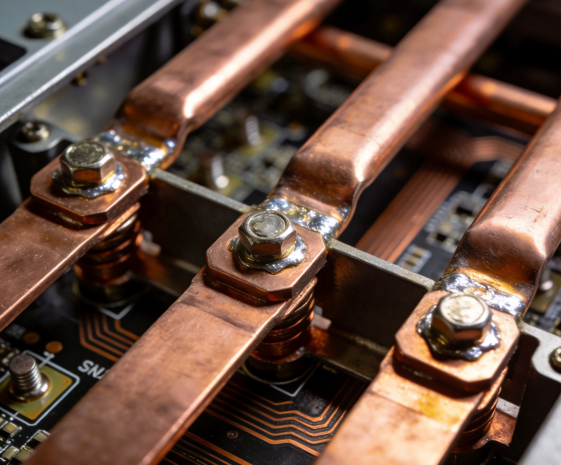
A typical renewable energy microgrid contains several Power Electronics nodes, each with distinct PCB requirements. The most current-intensive boards are found in the following system blocks:
Inverters that convert DC power from solar panels or battery storage into AC power for the microgrid must handle currents ranging from tens of amps in residential systems to hundreds or thousands of amps in commercial and industrial installations. At these current levels, Pcb Trace design alone is insufficient — bus bars, Heavy Copper planes, and sometimes discrete Bus Bar assemblies become necessary.
A BMS must measure cell voltages, manage charge balancing, and handle charge and discharge currents that can reach hundreds of amps in large storage systems. The main current-carrying PCB in a BMS handles the high-current path between battery cells and the system bus, requiring careful attention to contact resistance, thermal rise, and mechanical connector reliability.
Solar microinverters and string inverters use DC-DC boost stages to step up panel voltage before the inversion stage. These converters switch at high frequencies and must handle significant RMS current, placing demands on both the switching device packaging and the PCB's ability to manage both conduction losses and switching Loop Inductance.
Protection relays and grid-sensing circuits within a microgrid controller need to detect grid faults and disconnect the system within milliseconds. While these circuits do not carry high currents, they sit at the interface between the power electronics and the grid, requiring careful layout to avoid noise coupling into the measurement signals.
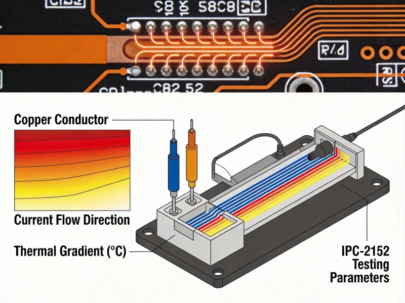
For currents above roughly 10 amps, most engineers reach for a trace width calculator based on Ipc-2152 or similar standards. These calculators are useful starting points, but in microgrid applications they are often insufficient on their own. The assumptions embedded in standard trace width charts — uniform temperature rise, still air, infinite heat spreading — do not reflect the actual thermal environment inside a microgrid enclosure.
In a multilayer board, outer layer traces have better Heat Dissipation through radiation and convection, but internal plane layers — when properly designed with thermal relief to planes — can carry significant current with less temperature rise than a comparable external trace because the entire copper plane acts as a heat spreader. For currents above 30 amps in continuous operation, moving to an internal Heavy Copper plane configuration is usually the right choice.
However, internal planes require careful thermal via placement if heat must be conducted to an external heatsink or thermal interface material. The thermal path from the high-current layer to the mounting surface must not be interrupted by clearance openings or keep-out zones that are too large.
When a single trace cannot carry the required current within the allowable temperature rise, splitting the current across two or more parallel traces on adjacent layers is a common approach. This requires ensuring that the current paths are balanced — equal resistance — so that neither trace carries a disproportionate share of the load. Vias connecting the parallel paths at both ends are critical for current sharing and must be sized and placed to avoid creating a high-resistance bottleneck at the via transition.
For currents above approximately 100 amps, discrete bus bars become the practical solution. A Bus Bar is a solid metal conductor — typically copper with tin or nickel plating — that replaces the PCB copper as the primary current-carrying element. The PCB in these designs still handles signal routing, gate drives, sensing, and control, but the high-current power path runs through the bus bar assembly.
Integrating bus bars with the PCB requires careful mechanical and Electrical Design. The interface between the bus bar and the PCB is typically a bolted connection or a soldered heavy-copper termination pad. Bolted connections must account for Thermal Cycling — the coefficient of thermal expansion (CTE) mismatch between Copper Bus Bar and FR4 substrate can loosen bolted connections over time if the clamp force and hardware specification are not chosen correctly. Soldered connections require heavy copper pad design with appropriate filleting to manage stress concentrations.
Microgrid power electronics operate in environments that can be thermally challenging. A solar installation in the southwestern United States or the Middle East may see ambient temperatures above 45 degrees Celsius, while an indoor battery storage installation may operate at elevated temperatures due to continuous charge-discharge cycling. Designing for thermal performance is not optional — it is a core part of the reliability engineering.
MOSFETs, IGBTs, and Schottky diodes in microgrid converters generate the majority of the heat on the board. The thermal path from the semiconductor junction to the ambient environment must be designed with explicit Thermal Resistance targets. This means selecting a heatsink with appropriate Thermal Resistance, specifying a thermal interface material (TIM) with the right thickness and thermal conductivity for the gap, and ensuring that the PCB itself does not become a thermal bottleneck.
When the switching device is on an internal layer of a multilayer board — which is common in bridge-leg configurations for noise reasons — Thermal Vias under the device package become essential for conducting heat to an external heatsink. The thermal via array must be designed with sufficient density and plating thickness to achieve the target thermal resistance without introducing voids that would degrade performance.
Heavy copper PCBs — boards with 3 oz/ft² or more copper on the power layers — are standard in microgrid inverter designs. The additional copper cross-section reduces resistive losses and spreads heat more effectively than thin copper. The trade-off is cost and, in some cases, increased difficulty in achieving fine feature resolution on signal layers that share the same board stack.
For most microgrid inverter designs, a hybrid approach works well: heavy copper on the inner Power Planes (2 to 4 oz/ft²), standard 1 oz/ft² copper on the signal and control layers, and careful design of the layer transition vias that connect the Power Planes to the switching devices.
Every microgrid PCB design has hotspots — locations where the temperature rise under full load exceeds the average board temperature by a significant margin. The corners of high-current pads, the junction of a trace and a via, and the area directly under a switching device are the most common culprits. Using thermal simulation during the design phase — tools like Ansys IcePak, Siemens FloTHERM, or even first-order analytical calculations — to identify these hotspots before the board is fabbed is strongly recommended.
The temperature budget for a microgrid PCB is the difference between the maximum expected ambient temperature and the maximum allowable junction temperature of the switching devices. If that budget is consumed by the base thermal resistance of the system, there is no headroom left for margin — and margin is what keeps systems running when conditions deviate from nominal.
The transition to wide-bandgap semiconductors — silicon carbide (SiC) MOSFETs and gallium nitride (GaN) HEMTs — in microgrid inverters has created new layout challenges and opportunities. These devices switch faster than silicon IGBTs and MOSFETs, which means that the parasitic inductance of the switching loop and the gate drive circuit has a much larger impact on switching losses and voltage overshoot.
The switching loop — the current path that carries the instantaneous load current during turn-on and turn-off of the switching device — must be as compact as possible in high-frequency microgrid converters. Every nanohenry of Loop Inductance at a switching frequency of 100 kHz or higher translates into additional voltage stress on the device and additional switching loss.
In PCB terms, minimizing switching loop inductance means placing the input capacitance as close as possible to the switching device, using wide and short traces or planes for the high-current loop, and keeping the gate drive return path separate from the power loop to avoid common-impedance coupling. In many SiC-based microgrid inverter designs, a dedicated DC link capacitor layer immediately adjacent to the switching device layer is used specifically to minimize this loop area.
SiC and GaN devices require gate drive circuits that can source and sink higher peak currents than traditional silicon MOSFET gate drives, because the gate charge must be delivered and removed faster to achieve the target switching speed. The gate driver IC should be placed as close to the switching device as possible, with short, wide traces for the gate and return connections.
Separate gate and sense Kelvin connections are standard practice in SiC designs. The Kelvin source connection removes the voltage drop of the power loop common-impedance from the gate loop, which becomes critical when the device is switching hundreds of amps and the voltage drop across the source inductance is non-trivial. Failure to implement Kelvin source connections in high-current SiC designs typically manifests as oscillation, spurious turn-on, or excessive ringing on the switching transients.
Microgrid power electronics require robust protection circuits to detect fault conditions and respond before damage occurs. The PCB must accommodate current sensing, voltage sensing, and temperature sensing circuits alongside the high-power switching circuitry without compromising the integrity of either.
Microgrid inverters and converters typically use hall-effect current sensors or shunt resistors for Current Measurement. Hall-effect sensors offer isolation and can measure high currents without the thermal loss of a shunt, but they add cost and introduce a small offset error and bandwidth limitation. Shunt resistors are lower cost and offer excellent bandwidth, but they dissipate power and require careful layout to avoid measurement error from temperature rise in the shunt itself.
For shunt-based current sensing, the Pcb Layout must ensure that the Kelvin sense connections are made at the actual resistor terminations, not at the Pcb Trace connection points. Any additional resistance between the resistor body and the sense point will create a measurement error that varies with load current and board temperature.
The short-circuit withstand capability of SiC MOSFETs in particular is a key design parameter for microgrid converters. A short circuit on the AC output of an inverter places the full DC link voltage across the switching device with the full short-circuit current flowing. The device must survive the short-circuit event long enough for the protection circuit to respond and turn the device off.
Pcb Layout directly affects the short-circuit current in a way that is sometimes overlooked. The loop inductance from the DC link capacitors to the switching device — the same loop that matters for switching loss — also determines how quickly the short-circuit current rises. A lower inductance loop means the short-circuit current rises faster, placing a tighter demand on the protection circuit's response time. Designing the DC link and switching loop layout for low inductance is thus important not only for efficiency but also for device protection.
Microgrid installations often operate in environments that are far from ideal. Dust, humidity, salt air, Thermal Cycling, and vibration are all common in real-world deployments. The PCB design must account for these conditions through material selection, conformal coating, and mechanical mounting provisions.
For microgrid hardware deployed outdoors, the base PCB material should be a high-Tg material (Tg above 150 degrees Celsius) to resist delamination during thermal cycling and high-humidity environments. Polyimide or high-Tg FR4 with enhanced moisture resistance ratings are common choices. If the design uses aluminum metal core or IMS (insulated metal substrate) for the power stage, the dielectric adhesive between the copper and the aluminum base must be rated for the maximum temperature and humidity exposure expected in the application.
PCBs in outdoor or high-humidity microgrid environments benefit significantly from conformal coating. An acrylic, urethane, or silicone conformal coating layer protects the board surface from moisture ingress, dust contamination, and surface arc tracking. The choice of coating type should account for the repairability requirement — some coatings are reworkable with specialized solvents, while others require baking to remove.
Large microgrid inverters are often wall-mounted or pole-mounted and experience vibration from wind loading or nearby equipment. The PCB mounting scheme should use standoffs or PEM studs to secure the board at multiple points, with attention to the location of heavy components like DC link capacitors that create a mass concentration. Reducing the board's resonant frequency through stiff mounting reduces the risk of fatigue failures in solder joints and connector terminations over a 15 to 20 year design life.
Designing PCBs for renewable energy microgrid power electronics demands a holistic approach that goes well beyond following a trace width calculator. The most critical design decisions — bus bar integration, Thermal Management architecture, switching loop layout, and protection circuit design — interact with each other and with the system-level thermal and mechanical environment in ways that cannot be optimized in isolation.
The transition to SiC and GaN wide-bandgap devices has raised the bar for PCB layout quality in microgrid converters. Layout choices that were acceptable at 20 kHz switching frequency are often completely unacceptable at 100 kHz or above. Investing in accurate thermal simulation, careful switching loop design, and robust protection architecture during the design phase pays dividends in system efficiency, reliability, and field support costs over the lifetime of the microgrid installation.
Contact us to discuss your requirements.
High Current PCB Design for High-Power LED DriversAugust/12/2026
A Deep Dive into High Current PCB Design for Solar InvertersJuly/17/2026
High Current PCB Design for Industrial Motor DrivesSeptember/28/2026
IPC-2152 Current Carrying Capacity Calculation GuideJune/03/2026
Designing a High Current PCB Motor Driver: Avoiding EMI PitfallsJuly/14/2026
High Current PCB Design for Aerospace Power DistributionSeptember/08/2026
High Current PCB Design GuidelinesMay/21/2026

High Current PCB Design for Railway Traction SystemsAugust/07/2026