

Aerospace Power Distribution systems place demands on Pcb Design that are fundamentally different from those of commercial electronics. A single board in an aircraft or spacecraft may need to carry hundreds of amps across bus bars, distribute power to avionics modules, motor controllers, lighting systems, and sensor arrays, all while operating across extreme temperature ranges, high vibration environments, and altitude-induced pressure variations. There is no margin for failure. The PCB is not just a substrate for components; it is critical infrastructure.
Designing High Current PCBs for aerospace applications requires a design philosophy that prioritizes reliability, redundancy, thermal robustness, and regulatory compliance above cost optimization. Decisions that might be acceptable in consumer electronics, such as minimizing Copper Weight to reduce material cost, or using the cheapest dielectric material that meets basic electrical requirements, are not permissible in aerospace Power Distribution designs. Every material choice, every Trace Width Calculation, and every Thermal Management decision must be traceable to a validated requirement and a known failure mode.
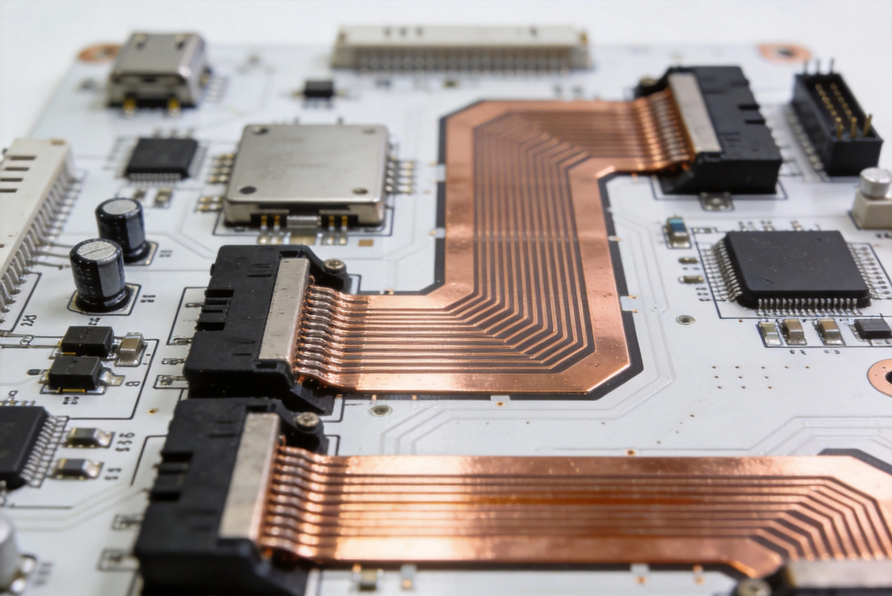
The foundation of High Current PCB design is accurate Current Carrying Capacity calculation. At currents above roughly 10 amps, the resistance of standard copper traces becomes significant. Power lost as heat (I squared R losses) accumulates, raising the board temperature. If the trace is not wide enough or the thermal path not adequate, the board will eventually exceed the glass transition temperature (Tg) of the substrate, leading to delamination, pad lifting, or solder joint failure.
The Ipc-2152 standard provides the authoritative reference for determining conductor current-carrying capacity in PCBs. Unlike older standards that used simplified formulas based on ambient temperature alone, Ipc-2152 accounts for the Thermal Resistance of the board, the Copper Weight, the presence or absence of internal planes, and whether the board is in free air or confined in an enclosure. For aerospace applications, which typically involve enclosed installations with limited airflow, the IPC-2152 enclosure correction factors are essential to accurate design.
At very high currents, above 50 or 100 amps, the design typically moves beyond trace routing to dedicated copper bus bars. Bus bars are flat copper strips, often 2mm to 5mm thick, that provide extremely low resistance paths for Current Distribution. In aerospace systems, bus bars are frequently incorporated into the PCB structure itself, using Heavy Copper layers or external copper bus bars that bolt directly to the board through Plated Through-hole terminals. The transition between the Bus Bar and the Pcb Traces requires careful thermal and mechanical design to avoid localized hot spots or joint failures under vibration.
Heavy Copper, defined as copper weights of 3oz per square foot (105 micrometers) or greater, is the standard approach for High Current routing in aerospace PCBs. Standard PCB Fabrication typically uses 1oz or 2oz copper. At 3oz, 4oz, or heavier, the trace width required for a given current drops significantly, but the fabrication challenges increase proportionally. Heavy copper boards require specialized lamination, drilling, and plating processes that not all manufacturers can reliably produce.
The PCB stack-up for aerospace power distribution must balance power routing needs with Signal Integrity requirements for any onboard electronics. A common approach is to dedicate entire internal layers to power distribution, with solid copper planes serving as both current carriers and thermal spreaders. The plane acts as a heatsink, distributing localized thermal loads across a wide area and reducing the temperature rise at high-current nodes.
For boards with extremely high current demands, hybrid constructions combining standard dielectric layers with metal-core or metal-backed sections are used. The metal core (typically aluminum or copper) provides superior thermal conductivity compared to FR-4, allowing heat to flow from power components to a chassis mount or external heat sink. These hybrid boards are more expensive and more complex to manufacture, but for the highest power densities in aerospace applications, they are often unavoidable.
Thermal Management in aerospace power PCBs is inseparable from reliability engineering. Components operating at elevated temperature degrade faster. The Arrhenius relationship states that for every 10 degrees Celsius increase in operating temperature, the failure rate of most electronic components roughly doubles. In an aerospace environment where maintenance intervals may be years apart and failure consequences are severe, thermal management is a direct contributor to system longevity and safety.
The primary thermal management tools for high current aerospace PCBs include Thermal Vias, metal backing plates, forced air cooling channels, and liquid cooling integration. Thermal Vias are the most common and lowest-cost approach. Arrays of Plated Through-hole vias placed directly under power components provide a low-thermal-resistance path from the component pad to an internal or external plane, spreading the heat across a wider area. The Thermal Via Array must be designed with adequate via density and plating quality to avoid becoming a thermal bottleneck.
For components exceeding 50 watts of dissipation, the design typically moves to direct metal backing. The PCB is mounted to an aluminum or copper plate that serves as both a mechanical support structure and a heat sink. Thermally conductive interface materials (TIMs) such as thermal pads or phase-change materials fill the microscopic air gaps between the PCB and the backing plate, improving thermal coupling. The interface quality between the board and the metal backing must be maintained throughout the board's service life, which in aerospace applications can span decades.
Where power densities exceed what air cooling can manage, liquid cooling integration becomes relevant. Some aerospace platforms use embedded micro-channel cooling structures within the PCB or the chassis, circulating coolant through passages that absorb heat directly from high-power components. These designs are complex and expensive but are used in high-power radar systems, electronic warfare platforms, and satellite Power Electronics where no other solution suffices.
Aerospace PCBs must operate in environments that would destroy commercial-grade materials. Altitude changes subject boards to rapid pressure cycling. Temperature swings from ground-level to cruising altitude can span 100 degrees Celsius or more. Vibration from engines, aerodynamic loads, and mechanical systems creates mechanical stresses that can fatigue solder joints and crack plating. UV exposure affects boards in exterior applications. Material selection must account for all applicable environmental factors.
The base laminate material for aerospace power PCBs is typically high-Tg FR-4 or a polyimide-based material. Standard FR-4 with a Tg of 130 to 140 degrees Celsius is insufficient for high-current aerospace applications where local temperatures can approach or exceed the glass transition point. High-Tg FR-4 (Tg above 170 degrees Celsius) provides significantly greater thermal margin. Polyimide (PI) and polyimide blends offer even higher thermal capability and better dimensional stability across temperature cycles, but at considerably higher cost and with more challenging fabrication requirements.
Beyond the base laminate, the prepreg and bonding film materials must be selected for their thermal conductivity, dielectric strength, and compatibility with the lamination process at heavy copper weights. Not all prepreg systems are rated for heavy copper lamination. The fabricator's engineering team should be involved early in the material selection process to ensure that the chosen laminate system is compatible with the required copper weights, layer count, and thermal performance targets.
Conformal coating is nearly universal in aerospace PCBs. An acrylic, urethane, or parylenene coating seals the board against moisture ingress, salt spray (in marine aviation applications), and contamination. For high current designs, conformal coating adds a secondary protection layer that can prevent tracking and surface corrosion on the board if the primary insulation is compromised. The coating type and thickness must be specified in the design documentation and verified during inspection.
Aerospace power distribution systems are designed with redundancy as a core architectural principle. Single points of failure are unacceptable in safety-critical systems. If one power bus fails, the system must continue operating on a backup bus. If one PCB fails, the load must be transferred to a secondary path. This requirement shapes the Pcb Layout in fundamental ways.
Redundant power distribution on a single PCB requires parallel current paths that are electrically isolated from each other under normal operation but can handle the full load if one path is interrupted. This means duplicate bus bars, duplicate plane layers, and duplicate output stages, all with appropriate fusing or solid-state protection devices. The Pcb Layout must ensure that a localized failure, such as a short circuit in one section, does not propagate to damage the redundant path.
Galvanic isolation between primary and redundant power domains is typically achieved through optocouplers, isolated gate drivers, or transformer-coupled converters. These isolation boundaries appear as physical gaps in the PCB layout, with separate copper regions that are electrically isolated but mechanically integrated. The gap width must be sufficient to withstand the full system voltage under all fault conditions, including transient overvoltages and partial discharge events at altitude.
Component derating is another form of redundancy embedded in the design. Aerospace standards such as MIL-HDBK-217Plus specify derating factors that require components to be operated at a fraction of their rated stress. A capacitor rated for 50 volts might be specified at 25 volts in an aerospace design. A connector rated for 10 amps might be rated at 5 amps. These derating margins provide safety margin against parameter drift, batch variation, and unexpected environmental stresses, reducing the probability of failure over the board's operational life.
High current switching in power distribution PCBs generates electromagnetic interference that can corrupt sensitive avionics signals or radiate beyond regulatory emission limits. The combination of high current, fast switching edges, and the close proximity of power and signal circuits in a multilayer aerospace board makes Emi control a central design challenge rather than an afterthought.
The primary Emi Mitigation techniques in high current aerospace PCBs are filtering, shielding, and careful layout. Input and output filters using feedthrough capacitors and common-mode chokes suppress conducted emissions on power connections. Shielded enclosures or local Shielding Cans around noisy circuits prevent radiated emissions from escaping the board. Shielding effectiveness depends on shield continuity, proper grounding, and the avoidance of apertures that act as slot antennas at the frequencies of interest.
Layout-driven Emi control focuses on controlling current loop areas and managing return paths. High current switching loops should be kept as small as physically possible, with the return path directly adjacent to the outbound path to minimize Loop Inductance. Ground planes must be continuous under switching circuits, with any slots or splits in the plane documented and justified. Via stitching along the edges of high-current traces provides a low-inductance return path and reduces radiated Loop Area.
Aerospace Emc Compliance is governed by standards such as MIL-STD-461 for conducted and radiated emissions and susceptibility, and DO-160 for aircraft equipment. These standards impose stringent limits on emission levels and require the board to operate correctly in the presence of radiated fields. Compliance testing is typically performed on the integrated system rather than on the PCB alone, but design decisions at the PCB level directly determine whether compliance is achievable.
Aerospace PCBs are regulated products subject to strict quality and process control requirements. The most widely referenced PCB specification is MIL-PRF-31032, which defines the performance and qualification requirements for printed circuit boards used in military and aerospace applications. Compliance with MIL-PRF-31032 requires the manufacturer to maintain a qualified process, use validated materials, and pass specific mechanical, electrical, and environmental tests.
Beyond MIL-PRF-31032, boards used in specific aerospace platforms must often comply with the prime contractor's detailed specifications. These may impose additional requirements on materials, hole sizes, minimum Annular Ring dimensions, surface finishes, and testing protocols. The Pcb Design must be developed with these specifications in mind from the earliest stages, as late discovery of a non-compliant material choice can require a complete redesign.
Traceability is a non-negotiable requirement in aerospace manufacturing. Every material lot, every process step, and every inspection result must be traceable to the individual board or batch. This traceability supports failure investigation, enables targeted recalls if a defect is discovered, and provides the documentation needed for airworthiness certification. PCB designs that do not support traceability are not acceptable for flight-critical applications, regardless of their electrical performance.
Aerospace power PCBs require more extensive testing than commercial boards. Beyond basic electrical continuity and insulation resistance testing, aerospace boards undergo Thermal Cycling, vibration testing, humidity testing, and in some cases, radiation testing for space applications. These tests verify that the board will survive the environmental conditions of its operational life without degradation.
High current testing involves passing the rated current through all power traces and bus bars while monitoring temperature rise. The board must reach thermal equilibrium, and no temperature measurement point may exceed the specified limit (typically 105 to 130 degrees Celsius depending on the application and material system). Thermal imaging during high current testing reveals hot spots that indicate localized resistance issues, insufficient thermal vias, or inadequate solder joints.
Destructive physical analysis (DPA) is performed on sample boards to verify internal construction quality. Cross-sections of vias, layer-to-layer registration, plating quality, and laminate voids are all evaluated under microscopy. DPA is typically performed on production boards and on boards that have undergone environmental testing, to verify that the board's internal structure has not degraded under thermal or mechanical stress.
Designing high current PCBs for aerospace power distribution is a discipline that combines Electrical Engineering, thermal physics, materials science, and regulatory compliance into a single, demanding practice. The boards must carry hundreds of amps reliably across extreme temperature ranges and decades of service life, in systems where failure is not an option. Every design decision, from copper weight to laminate selection to thermal via placement, must be made with explicit consideration of its impact on reliability, safety, and airworthiness.
The engineers who produce the most successful aerospace power PCBs are those who treat the fabricator as a partner from the earliest stages, involve reliability and compliance specialists in the design process, and maintain rigorous traceability throughout. The cost and complexity of aerospace PCB development is high, but it is justified by the critical role these boards play in the safety and functionality of aerospace platforms worldwide.
Aerospace high current power PCBs typically use 3oz to 6oz copper weight on power layers, with some designs going to 10oz or heavier for Bus Bar integration. The specific requirement depends on the current magnitude, acceptable temperature rise, and board layout constraints. For currents above 100 amps, designers often transition from etched traces to bolted copper bus bars rather than relying on trace routing alone.
MIL-PRF-31032 is a military performance specification for printed circuit boards that defines material requirements, construction standards, electrical and mechanical test methods, and quality assurance provisions. Boards manufactured to MIL-PRF-31032 are accepted by most aerospace prime contractors as meeting a recognized quality baseline. It is the most commonly specified PCB standard in aerospace and defense programs.
Aerospace PCBs experience large temperature cycles that cause the board and the components to expand and contract at different rates due to their different coefficients of thermal expansion (CTE). Mitigation strategies include using polyimide or hybrid materials with lower CTE mismatch to copper, underfilling or staking components to distribute stress, using flexible sections in the board to accommodate differential expansion, and selecting components with leads or solder joints that can accommodate the differential movement.
Electroless Nickel Immersion Gold (Enig) is the most common Surface Finish for aerospace boards due to its flatness, corrosion resistance, and shelf life stability. Hard gold plating over nickel is used on contact surfaces and edge connectors. For high current applications where solderability must be maintained over long periods, Enig or Immersion Silver are preferred over Hasl, which can introduce unevenness on fine-pitch features.
Commercial Off-The-Shelf (COTS) components may be used in aerospace applications where they meet the program's derating and environmental requirements and where the consequence of failure is acceptable. Many aerospace programs use COTS components in non-safety-critical functions. For safety-critical power distribution, components with established flight heritage, full traceability documentation, and screening to applicable standards (such as MIL-SPEC screening or DESC drawings) are typically required.
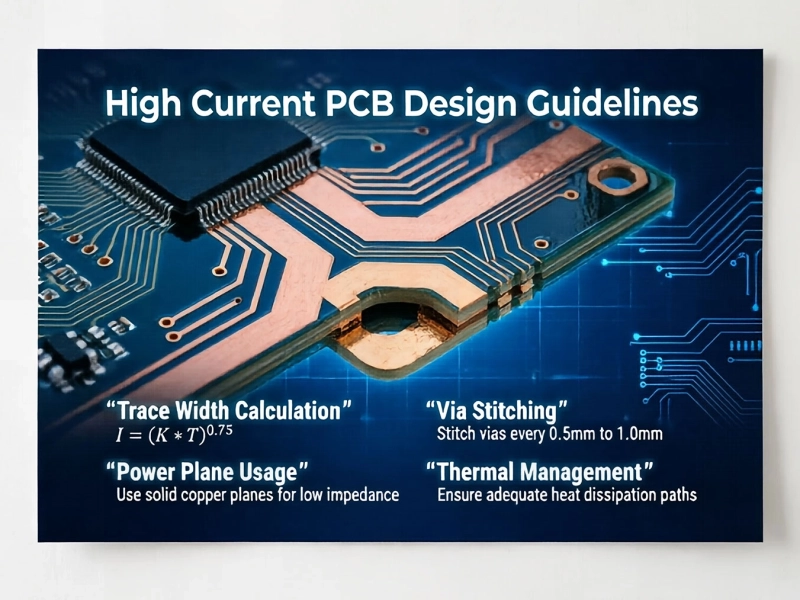
High Current PCB Design Guidelines: Ensuring Reliability and SafetyJune/08/2026
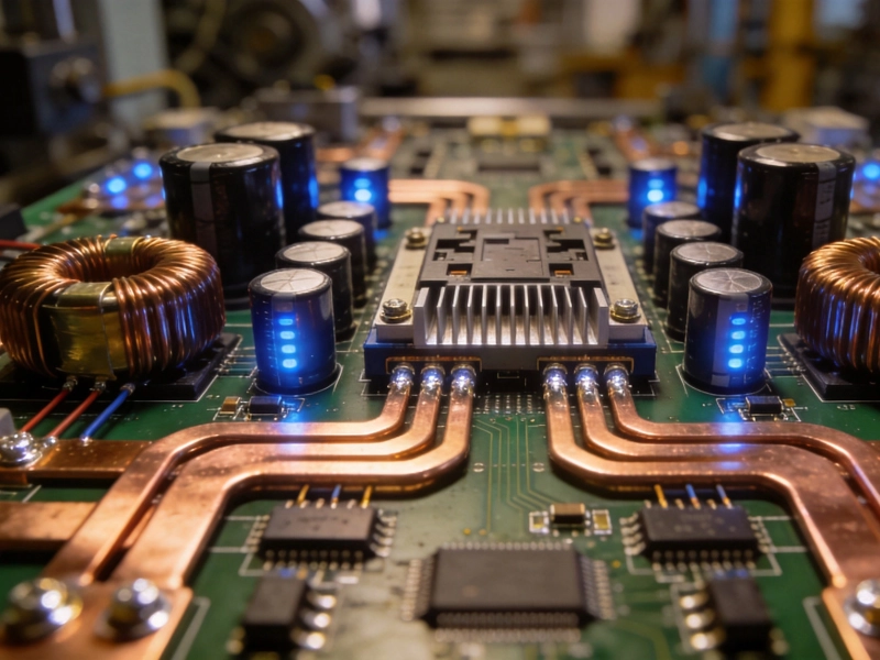
High Current PCB Design for Industrial Motor DrivesSeptember/28/2026
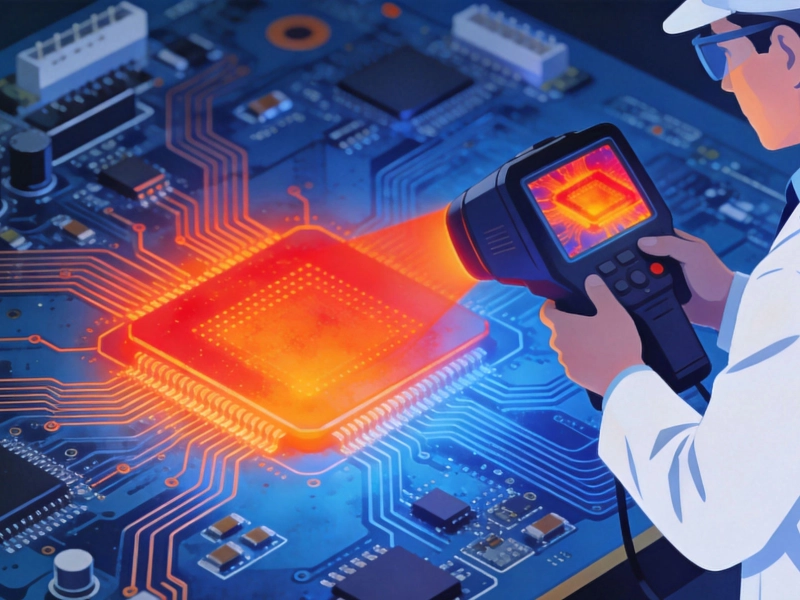
5 Critical Thermal Management Problems in High Power PCBsMay/21/2026
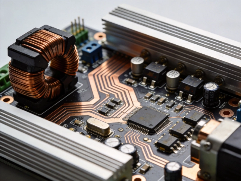
High Current PCB Design for Robotics Motor ControllersSeptember/16/2026
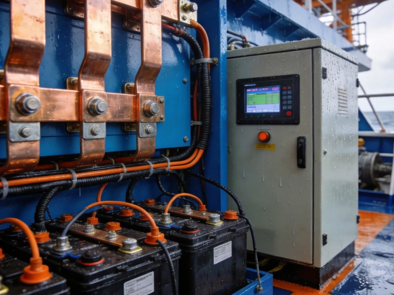
High Current PCB Design for Marine Battery SystemsSeptember/21/2026
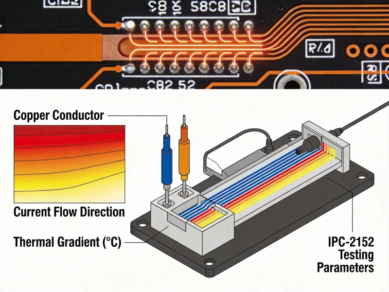
IPC-2152 Current Carrying Capacity Calculation GuideJune/03/2026
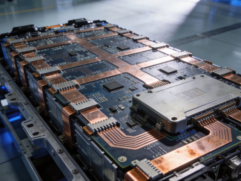
Designing a 100A High Current PCB for EV Battery Management SystemsJuly/09/2026

High Current PCB Thermal Relief: Full Connect vs. Modified SpokesJuly/16/2026