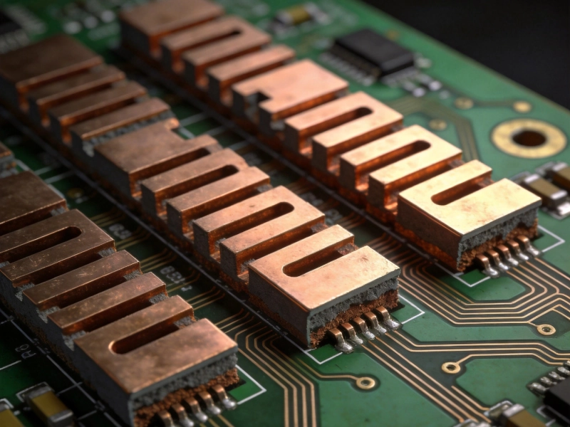
Power delivery is the unsung backbone of every electronic system. While signal integrity and high-speed routing get the spotlight, the connectors that carry tens or hundreds of amperes into and out of a PCB determine whether a design runs cool and reliable or overheats and fails. High-current Pcb edge connectors—card-edge gold fingers, right-angle power headers, and bus-bar interconnects—are the critical interface between power supplies, backplanes, and daughter cards in industrial, telecom, and automotive applications. Understanding their current ratings and thermal limits is not optional; it is the difference between a system that survives its rated lifetime and one that fails under worst-case conditions.

What Defines a High-Current Edge Connector?
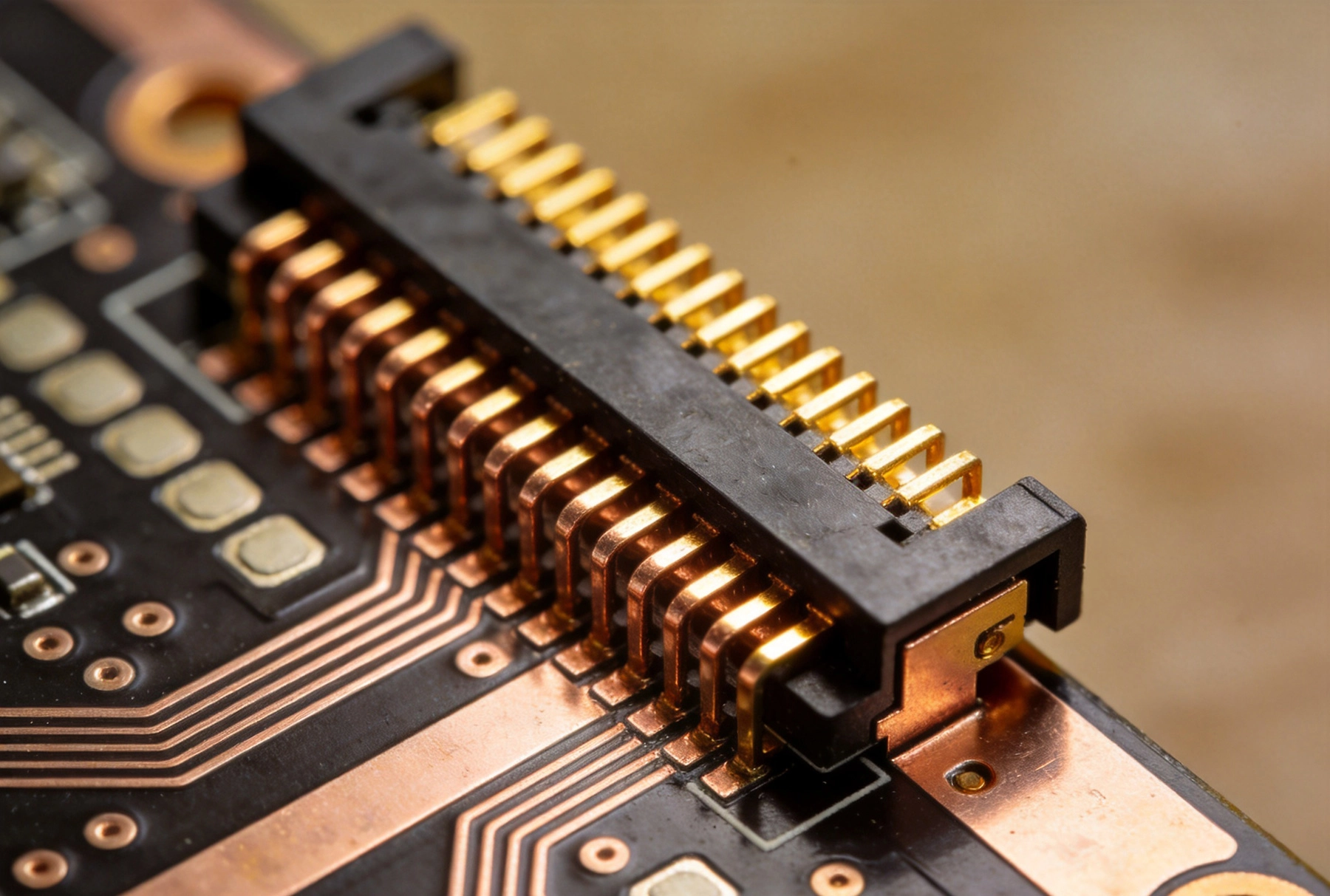
Edge connectors differ from standard through-hole or surface-mount headers in one fundamental way: the PCB itself becomes half of the connector. Copper traces on the board edge are plated with gold over nickel to form contact fingers that mate with a receptacle on the opposing board or chassis. This architecture offers several advantages for Power Distribution:
- Zero insertion-loss interconnect. There is no separate contact pin and socket—just a direct metal-to-metal wipe between the PCB finger and the receptacle contact. Contact resistance is typically below 5 mΩ per finger.
- High pin density with shared power. Multiple fingers can be ganged in parallel to multiply current capacity without adding connector height.
- Space efficiency. The connector sits at the board edge, consuming no interior routing area—ideal for backplane and rack systems where board real estate is scarce.
- Serviceability. Daughter cards can be hot-swapped without disconnecting cables or unsoldering joints.
But those advantages come with a catch: the current capacity of an edge connector is not a single number you look up in a datasheet. It depends on a web of interacting factors—finger geometry, Copper Weight, plating thickness, ambient temperature, airflow, mating cycles, and the Thermal Resistance of the PCB itself. Getting any one of these wrong can lead to localized overheating that is invisible to system-level thermal simulations.
Current Rating Fundamentals: It Is Always Thermal
There is no such thing as a "purely electrical" current rating. Every ampere that flows through a conductor generates heat (I²R losses), and the current rating is simply the current at which the resulting temperature rise reaches an acceptable limit. The three reference points that matter are:
- Mate temperature. The contact interface temperature where the gold-plated finger meets the receptacle. Exceeding ~125 °C at the interface risks degrading the gold plating, accelerating fretting corrosion, and increasing contact resistance—a positive-feedback loop that ends in thermal runaway.
- Pcb Trace temperature. The temperature of the Copper Trace feeding the edge finger. Ipc-2152 defines allowable temperature rises above ambient for internal and external conductors, but these are conservative norms, not failure boundaries. Lamination degradation and solder-mask discoloration typically begin around 130–140 °C for standard FR-4.
- Component vicinity temperature. Solder joints of nearby components must stay within their rated operating range. A 20 A finger running at 30 °C above ambient can push adjacent SMD components beyond their limits even if the finger itself is fine.
Designers must evaluate all three temperatures simultaneously. Optimizing finger geometry alone is insufficient if the Pcb Trace feeding it is a bottleneck.
Finger Geometry and Copper Weight
Finger Width and Thickness
Current capacity scales roughly with the cross-sectional area of the conductor. For edge connectors, this means:
- Finger width. Standard signal fingers are 0.5–1.0 mm wide. High-current fingers are typically 2.0–5.0 mm wide, often occupying the same pitch but merging adjacent signal positions into a single wide power finger.
- Copper Weight. Standard 1 oz copper (35 µm) is inadequate for currents above ~5 A per finger. High-current edge connectors use 2 oz (70 µm), 3 oz (105 µm), or even 4 oz (140 µm) copper on the outer layers. Each doubling of Copper Thickness roughly doubles the current capacity for a given temperature rise.
- Plating stack. Electroplated nickel (2–5 µm) under hard gold (0.5–1.3 µm) is standard. The nickel barrier prevents copper migration into the gold; the hard gold provides wear resistance for multiple mating cycles. For very High Current (>30 A per finger), some designs add a thick soft-gold overplate (2–5 µm) to reduce contact resistance, accepting reduced wear life in exchange.
The Parallel-Finger Strategy
When a single finger cannot carry the required current, the standard approach is to gang multiple fingers in parallel. This is effective but not as simple as dividing the total current equally among N fingers:
- Current sharing imbalance. Small differences in contact resistance (±2 mΩ is typical across a batch) cause unequal Current Distribution. The hottest finger carries more than 1/N of the total current. A conservative derating factor of 0.8–0.9 per parallel finger is recommended.
- Thermal coupling. Adjacent fingers heat each other. Two 3 mm fingers on 2 mm pitch share thermal mass, so the per-finger current derating is more severe than two isolated fingers on 10 mm pitch.
- Mating sequence. If one finger mates before its neighbor (due to card-edge bevel or connector stagger), it carries full current for the brief moment before the second finger engages. This "first-mate" current spike can exceed the finger's steady-state rating if the total current is high and the mating time difference is long enough for thermal inertia to be insufficient.
A practical rule: for N parallel fingers, derate total capacity to 0.85 × N × I_single for closely spaced fingers (pitch ≤ 3 mm), and 0.9 × N × I_single for widely spaced fingers (pitch ≥ 6 mm).
Thermal Limits: From Finger to System
Conduction Through the PCB
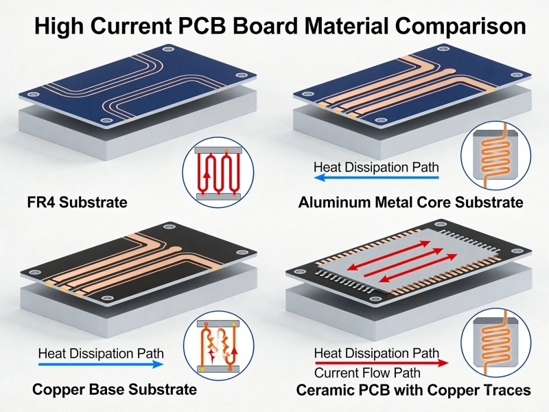
Heat generated at the edge finger conducts into the PCB through the Copper Trace and spreads laterally through copper planes. The thermal conductivity of copper (~385 W/m·K) is excellent, but the dielectric layers between copper have much lower conductivity (~0.3 W/m·K for FR-4). This means:
- Heat spreads efficiently within a copper layer but poorly between layers.
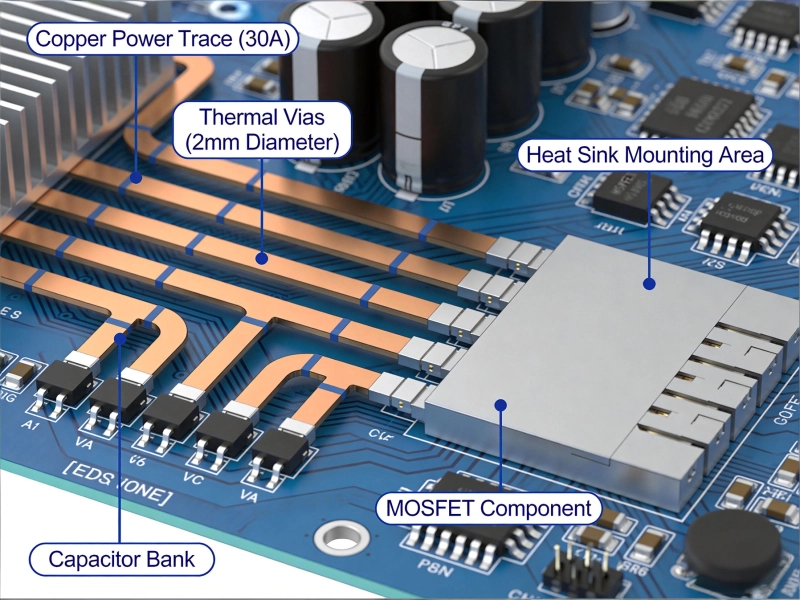
- Inner copper planes (ground and power) act as heat spreaders only if they are connected to the finger layer through Thermal Vias. A typical thermal-via array under a high-current pad uses 0.3 mm vias on 1.0 mm pitch, filled with copper or solder to maximize cross-sectional area.
- Board thickness matters. A 1.6 mm board has a longer thermal path from outer layer to inner planes than a 0.8 mm board, but the thinner board has less copper volume and lower thermal mass.
Convection and Airflow
In sealed enclosures with no forced airflow, convection from the PCB surface is the primary heat-removal mechanism. The natural-convection coefficient for a horizontal PCB is typically 5–10 W/m²·K—barely enough to remove the heat from a 15 A finger running 20 °C above ambient. Forced-air cooling transforms the picture:
- 1 m/s airflow increases the convection coefficient to ~25 W/m²·K, roughly tripling the sustainable current for a given temperature rise.
- 2–3 m/s (typical of fan-cooled telecom racks) enables 4–5× the natural-convection current.
But airflow direction matters. Air flowing parallel to the board edge cools the fingers directly; air flowing perpendicular may create a stagnation zone at the connector. System-level CFD simulation is the only reliable way to predict connector temperatures in complex enclosures.
Radiation
Radiation cooling is often neglected in PCB Thermal Analysis but becomes significant at high temperature rises. A connector finger at 100 °C in a 40 °C ambient radiates approximately 30–40 W/m²—small compared to forced convection but meaningful in sealed, fanless systems. The emissivity of the surface matters: gold plating has very low emissivity (~0.02–0.05), while solder mask and dark PCB laminate have higher emissivity (~0.85–0.95). Exposing bare copper or solder mask around the connector area improves radiation cooling.
IPC and Industry Standards for Current Rating
Several standards provide current-rating guidance, but each has limitations that designers must understand:
- Ipc-2152 (Standard for Determining Current-Carrying Capacity in Printed Board Design): Provides empirical curves for conductor temperature rise as a function of cross-sectional area, with modifiers for internal vs. external conductors and board thickness. It is the most widely used standard but was developed for traces, not edge-connector fingers. The contact-resistance heating at the finger interface is not captured.
- Ipc-2221 (Generic Standard on Printed Board Design): Contains current-capacity curves that are simpler and more conservative than IPC-2152, but are based on older data and can be overly restrictive for high-copper-weight designs.
- MIL-DTL-55302 (Edge-Card Connectors): Specifies current ratings for military-grade edge-card connectors, typically 3 A per contact at 25 °C ambient. These ratings are for the receptacle contact, not the PCB finger, and assume specific mating conditions.
- IEC 60512-5-1 (Test Schedule for Connectors — Current-Carrying Capacity): Defines the test method for measuring current-carrying capacity by monitoring temperature rise at the contact interface. This is the most rigorous way to establish a rating but requires physical test hardware.
No single standard covers the complete picture of a PCB edge connector. The best practice is to use IPC-2152 for the PCB trace portion, add the I²R heating from contact resistance (measured or from the connector datasheet), and verify the combined temperature against the plating and laminate limits through testing or simulation.
Design Guidelines for High-Current Edge Connectors
Copper and Plating
- Use 2 oz or 3 oz copper on the finger layer for currents above 10 A per finger.
- Specify hard gold over electroplated nickel (Ni 3–5 µm / Au 0.8–1.3 µm) for mating cycles ≤ 200. Use thicker soft gold (Au 2–5 µm) for very High Current or low contact-resistance requirements, with mating cycles ≤ 50.
- Extend Copper Thickness beyond the finger into the feed trace. A 3 oz finger feeding into a 1 oz trace creates a thermal bottleneck at the transition.
Trace Routing
- Feed the finger with the widest practical trace—ideally the same width as the finger for at least 5 mm from the edge. Taper transitions gradually (no abrupt width changes).
- Use copper pours connected to the power trace on the same layer to increase effective cross-section and heat spreading.
- Place Thermal Vias (0.3 mm, 1.0 mm pitch, filled) under and around the finger pad to conduct heat to inner planes.
Finger Layout
- Group power fingers together at one end of the edge connector, away from high-speed signal fingers, to minimize thermal impact on signal integrity.
- Provide at least 2× finger-width spacing between adjacent power fingers to reduce thermal coupling and current-sharing imbalance.
- Place ground fingers on both sides of each power finger group to provide both electrical shielding and a thermal heat-spreading boundary.
Thermal Management at the System Level
- Ensure forced airflow across the connector area whenever possible. Even 0.5 m/s makes a significant difference in sustainable current.
- If the connector is in a sealed enclosure, use thermal interface material (TIM) between the PCB and a metal chassis wall to conduct heat out of the board.
- Consider bus-bar augmentation: a copper or aluminum Bus Bar soldered or screwed to the PCB near the edge connector can carry the bulk of the current, with the edge connector handling only the mating interface.
Common Failure Modes and How to Avoid Them
- Thermal runaway at the contact interface. Increased contact resistance → more I²R heating → higher temperature → oxidation/fretting → even higher resistance. Prevention: stay below 100 °C at the interface, use adequate gold plating, and ensure minimum normal force per the connector specification (typically 50–150 g per contact).
- Trace burnout at the finger-to-trace transition. A narrow trace feeding a wide finger is a fuse. Prevention: match trace width to finger width or use copper pours to spread the cross-section.
- Solder-mask cracking. Repeated Thermal Cycling cracks solder mask over high-current traces, exposing copper to contamination and potential shorts. Prevention: specify solder-mask opening (SMD) over high-current fingers, or use high-Tg solder mask rated for >130 °C continuous.
- Lamination delamination. If the PCB temperature near the edge connector exceeds Tg (glass-transition temperature) of the laminate, the epoxy softens and layers separate. Prevention: use high-Tg laminate (Tg ≥ 170 °C) for boards carrying >20 A per finger, and keep operating temperature at least 25 °C below Tg.
- Gold plating wear. Each mating cycle removes ~10–30 nm of hard gold. After 200 cycles, the gold may be thin enough for nickel exposure, increasing contact resistance and corrosion susceptibility. Prevention: specify thicker gold for high-cycle applications, or use alternative contact finishes such as palladium-nickel or silver-palladium.
Testing and Verification
No design is complete without validation. Recommended tests for high-current edge connectors include:
- Steady-state temperature measurement. Apply rated current and measure contact-interface temperature using thermocouples (≤36 AWG wire, bonded with high-thermal-conductivity adhesive) or infrared thermography with emissivity correction. Verify that all temperatures are within limits at worst-case ambient temperature and minimum airflow.
- Current-sharing verification. For parallel fingers, measure current in each finger using a Hall-effect probe or Shunt Resistor. Confirm that no single finger carries more than 1.1 × (I_total / N).
- Thermal Cycling. Cycle the connector between −40 °C and +85 °C (or the application's temperature range) for 500+ cycles, then re-measure contact resistance. A >20 % increase indicates plating degradation.
- Mating-cycle endurance. Mate and unmate the connector for the rated number of cycles, measuring contact resistance every 50 cycles. Plot the trend to project end-of-life resistance.
- Overcurrent survival. Apply 1.5× rated current for 1 hour and verify that no permanent degradation (resistance increase >5 %, visual damage, or outgassing) occurs.
Choosing a PCB Fabricator for High-Current Edge Connectors
Not every PCB house can reliably manufacture high-current edge connectors. Key capabilities to verify:
- Heavy Copper capability. 3 oz and 4 oz outer-layer copper require specialized etching processes. Standard 1 oz etch lines cannot achieve the tight dimensional tolerances needed for edge fingers.
- Edge plating (castellated holes or wrap-around plating). If the design calls for plated edges rather than separate fingers, the fabricator must have edge-plating capability with controlled plating thickness.
- Gold plating control. Verify that the fabricator can meet both thickness and hardness specifications for the gold overplate, with XRF fluorescence measurement on production panels.
- Impedance and continuity testing. High-current fingers should be tested for continuity and isolation at final electrical test. Thermal-relief via structures should be verified by cross-section.
- IPC-A-600 acceptability. Class 3 acceptance criteria for edge-contact plating—no exposed nickel, no plating skips, minimum 0.5 mm plating length from the board edge.
Conclusion
High-current Pcb edge connectors sit at the intersection of electrical, thermal, and mechanical engineering. Their current rating is not a datasheet number to be looked up and applied blindly—it is a system-level outcome that depends on copper weight, finger geometry, plating quality, Pcb Thermal Design, enclosure cooling, and operating conditions. The most dangerous design error is treating the connector in isolation: a finger that is perfectly rated in free air may fail catastrophically inside a sealed enclosure with no airflow, or when fed by a trace that is half its width.
Successful high-current edge-connector design requires thinking in three dimensions: the conductor cross-section (copper weight × finger width), the thermal path (trace, vias, inner planes, and enclosure), and the contact interface (plating, normal force, and mating cycles). When all three are co-designed and verified through testing, the result is a power interconnect that runs cool, mates reliably, and delivers its rated current for the life of the product.
For assistance with high-current Pcb Design, edge-connector specification, or thermal validation, contact our engineering team to discuss your requirements.
FAQ
How much current can a single PCB edge finger carry?
It depends on finger width, copper weight, plating, and cooling. A typical 3 mm wide finger on 2 oz copper can carry 10–15 A with a 20–30 °C temperature rise in natural convection. With forced airflow and 3 oz copper, the same finger may handle 20–25 A.
Why do parallel fingers not share current equally?
Small variations in contact resistance (±1–3 mΩ) across fingers cause unequal Current Distribution. The finger with the lowest resistance carries the most current and runs the hottest. A derating factor of 0.85–0.9 per parallel finger accounts for this imbalance.
What copper weight should I use for high-current edge connectors?
For currents above 10 A per finger, 2 oz (70 µm) copper is the minimum. For 20+ A per finger or high ambient temperatures, 3 oz (105 µm) or 4 oz (140 µm) is recommended. The feed trace should match the finger's copper weight to avoid a thermal bottleneck.
What happens if the edge connector overheats?
Overheating degrades the gold-nickel plating, increases contact resistance, and can trigger thermal runaway—where rising resistance causes more heating, which raises resistance further. In extreme cases, the laminate delaminates or the solder mask cracks, potentially causing catastrophic failure.
How do I verify the current rating of my edge-connector design?
Build a test board with thermocouples at the contact interface and on the feed trace. Apply rated current at worst-case ambient temperature and minimum airflow, and measure steady-state temperatures. Also test current sharing across parallel fingers and thermal-cycling endurance to verify long-term reliability.