

High-voltage direct current (HVDC) transmission is experiencing a renaissance. As renewable energy sources—particularly offshore wind and remote solar farms—push power generation farther from population centers, HVDC's superior long-distance efficiency over AC transmission makes it the technology of choice for moving gigawatts across hundreds of kilometers. At the heart of every HVDC converter station are Power Electronics modules that handle enormous currents at extreme voltages, and the printed circuit boards within these modules must survive electrical and thermal stresses that would destroy a conventional board in seconds.
Designing PCBs for high-current, high-voltage DC transmission applications requires a fundamentally different mindset than standard electronics design. The rules that govern low-voltage digital boards—minimum trace widths defined by current-carrying capacity alone, clearances measured in a few mils—do not apply. Instead, you must simultaneously manage thermal dissipation, voltage isolation, partial discharge resistance, and mechanical integrity under extreme conditions.
This article covers the critical design principles, material considerations, and layout techniques that make high-current PCBs reliable in high-voltage DC transmission environments.
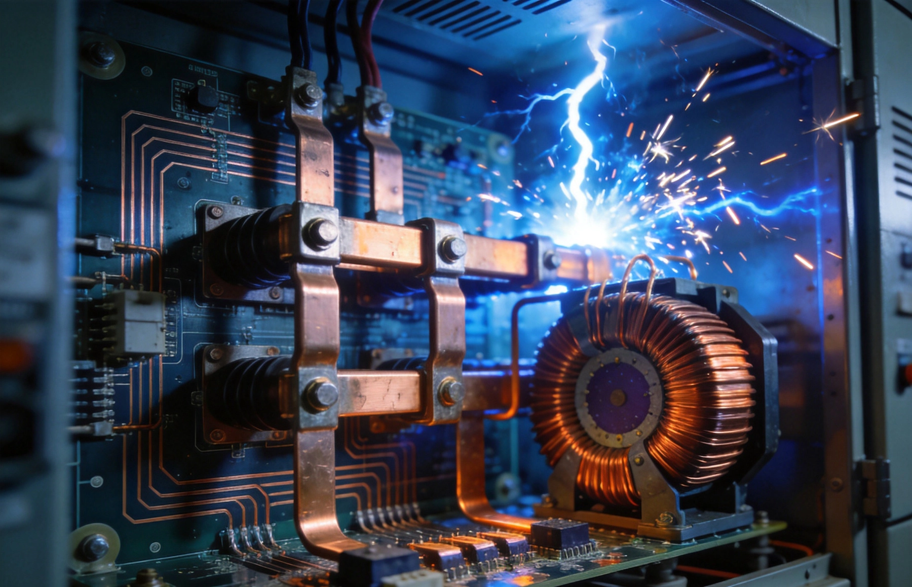
Before diving into design rules, it is essential to understand what the PCB must withstand. HVDC converter stations typically operate at DC voltages ranging from ±150 kV for back-to-back converters to ±800 kV or even ±1100 kV for ultra-long-distance transmission. The PCBs within these systems do not see the full transmission voltage—they are typically in the valve hall electronics, gate driver circuits, monitoring systems, and DC-link capacitor banks—but they can still face voltages of several kilovolts and currents of hundreds or thousands of amperes.
Unlike AC systems where voltage periodically returns to zero, DC voltage is continuous. This means insulation is under constant electrical stress, which accelerates several failure mechanisms:
Even in nominally DC systems, transients occur. Switching events in the converter valves generate voltage steps with rise times in the microsecond range. Fault conditions can impose surge voltages many times the nominal DC level. Lightning strikes on the DC transmission line can propagate surges into the converter station. The PCB insulation must withstand not just the steady-state DC voltage but these superimposed transients without breaking down.
In high-voltage design, the distance between conductors at different potentials is the single most important parameter determining reliability. Two distinct distances matter:
Under DC voltage, creepage distances are typically larger than for equivalent AC voltages because the constant electrical stress promotes surface contamination-driven tracking more aggressively. IEC 60664-1 provides the foundational standard for insulation coordination, but for HVDC applications, additional guidance comes from IEC 60815 (creepage distances for DC) and the applicable equipment standards (IEC 62920 for wind turbine converters, IEC 61800 for power converters, etc.).
The required creepage distance depends on the voltage, the pollution degree of the environment, and the comparative tracking index (CTI) of the insulating material. For HVDC valve hall electronics (pollution degree 2, overvoltage category III), creepage distances of 8-16 mm per kilovolt of working voltage are typical, depending on the material's CTI rating.
The CTI of the PCB laminate directly determines the creepage multiplier. Standard FR-4 has a CTI of 175V (Material Group II), requiring relatively large creepage distances. High-CTI materials—such as certain polyimides or specially formulated epoxy systems with CTI ratings above 600V (Material Group I)—allow significantly reduced creepage distances for the same voltage, which can be crucial for space-constrained designs.
For the highest-voltage PCB sections, slotting or grooving the board between high-voltage conductors can effectively increase the creepage path without consuming additional board area. The slot forces the potential to track along the board surface and around the slot, roughly doubling the creepage distance for a given spatial separation.
High-current PCBs for HVDC applications use copper weights far beyond standard 1 oz (35 µm) foil. Heavy Copper PCBs—defined as boards using 3 oz (105 µm) or thicker copper per layer—are essential for carrying the hundreds or thousands of amperes involved in DC transmission power stages.
The required Copper Weight depends on the maximum current, the allowable temperature rise, and whether the trace is on an internal or external layer. Internal layers dissipate heat less efficiently because they are surrounded by dielectric material rather than exposed to air, so they require wider traces or heavier copper for the same current.
For HVDC power modules, common copper weights include:
These current-carrying capacities are approximate and must be verified using Ipc-2152 calculations that account for the specific Trace Geometry, board stackup, and thermal environment of your design.
For high-current paths, broad copper pours connected by multiple vias (via arrays or via stitching) are generally preferred over individual traces. Copper pours provide lower inductance—critical for the high di/dt associated with IGBT switching—and better thermal spreading across the board. The pours also serve as heat spreaders, conducting heat from power devices to the board surface where it can be transferred to heatsinks or the surrounding air.
Heavy Copper creates a significant lamination challenge. If one layer has 10 oz copper while the opposing layer has only 1 oz, the asymmetric copper distribution causes the board to warp during lamination and reflow. This warpage can prevent proper contact with heatsinks, cause BGA solder joint opens during reflow, and create mechanical stress on through-hole components.
The solution is Copper Balancing—adding non-functional copper (copper thieving) on signal layers to match the copper distribution on heavy-copper power layers. The goal is to maintain approximately equal copper area on opposing sides of the board core at every layer pair.
Material selection is critical for HVDC PCBs. The dielectric must resist not only the steady-state DC voltage but also the long-term degradation mechanisms that DC stress accelerates.
For the voltage levels encountered in HVDC converter electronics, the PCB laminate must have a CTI rating appropriate for the creepage distances in the design. Standard FR-4 (CTI 175V) may be adequate for lower-voltage sections (gate driver logic, control electronics), but the power sections require high-CTI materials. Options include:
Partial discharge (PD)—small electrical discharges that occur in voids or at interfaces within the insulation—is the primary long-term degradation mechanism for HVDC insulation. Each PD event erodes the insulating material slightly; over thousands of hours, this erosion can grow until it bridges the entire insulation thickness, causing complete breakdown.
Under DC voltage, PD is less frequent than under AC (because the electric field is static, not continuously reversing) but each PD event is more damaging because the same location is stressed in the same direction every time. PCB laminates with fewer voids, better resin flow during lamination, and higher breakdown strength per unit thickness provide superior PD resistance.
Water absorption is a critical concern for HVDC PCBs because water both reduces the volume resistivity of the dielectric (increasing leakage current) and promotes CAF growth along glass fiber bundles within the laminate. Materials with moisture absorption rates below 0.1% by weight are strongly preferred for HVDC applications. After fabrication, boards may require conformal coating or potting to prevent moisture ingress during service.
High-current PCBs for HVDC systems generate substantial heat—not just I²R losses in the copper but also switching losses in the power semiconductors, core losses in magnetic components, and ripple current losses in DC-link capacitors. Managing this heat is essential for both reliability and performance.
Thermal Vias—plated through-holes placed in arrays beneath power component pads—provide a low-resistance thermal path from the component attachment layer to internal copper planes or the opposite board surface. For HVDC applications, thermal via arrays must be designed carefully:
For the highest-power sections—IGBT modules, diode modules, and Bus Bar interfaces—insulated metal substrate (IMS) boards, also known as metal core PCBs (MCPCBs), offer thermal conductivity 5-10 times better than standard FR-4. The thin dielectric layer (typically 75-200 µm of ceramic-filled epoxy or polyimide) provides electrical isolation while minimizing the thermal resistance between the copper circuit layer and the aluminum or copper baseplate.
In HVDC applications, the dielectric layer in IMS boards must be carefully evaluated for PD resistance, CTI, and long-term reliability under DC stress. Not all IMS dielectrics are suitable for high-voltage DC operation.
The PCB-to-heatsink interface is a critical thermal bottleneck. The board must maintain flatness despite heavy copper content and Thermal Cycling, and the thermal interface material (TIM) must maintain consistent performance over the equipment's 25-30 year service life. Thermal pads with controlled thickness and compliance are preferred over thermal greases, which can pump out under thermal cycling or dry out over decades.
Layout is where all the design principles converge. A well-executed layout can make even marginal materials perform reliably, while a poor layout can cause failures even with the best materials.
The most effective layout strategy for HVDC PCBs is to organize the board into voltage zones, with the highest-voltage sections physically separated from low-voltage control circuitry. This zoning minimizes the risk of voltage stress on components not rated for high voltage and reduces the board area that requires high-CTI materials and large creepage distances.
Typical zones include:
Keep the zones physically separated with guard traces (at earth or neutral potential) between high-voltage and low-voltage areas to intercept any surface contamination or creepage paths.
High di/dt in IGBT switching transients—currents that change by hundreds of amperes in tens of nanoseconds—demands extremely low Loop Inductance in the power path. Even 10 nH of stray inductance can generate voltage spikes of hundreds of volts during turn-off, potentially exceeding the IGBT's voltage rating.
Layout techniques to minimize Loop Inductance include:
Snubber circuits (RCD clamps) absorb switching energy and limit voltage overshoot. Their effectiveness depends critically on layout—the snubber must be connected with minimal inductance between the IGBT collector and emitter. Place snubber components immediately adjacent to the IGBT module terminals with short, wide copper connections. A poorly laid-out snubber with long traces can actually worsen the voltage overshoot by adding its inductance to the circuit.
In the harsh environment of an HVDC valve hall—where high electric fields, temperature cycling, humidity, and contamination are all present—conformal coating or potting provides an essential additional layer of protection.
For HVDC PCBs, the coating must provide:
Parylene conformal coating is often the premium choice for HVDC applications due to its exceptional dielectric strength (7000 V/mil), pinhole-free conformal coverage, and outstanding moisture barrier properties. Silicone coatings offer good thermal cycling resistance but lower dielectric strength. Epoxy coatings provide hard, chemically resistant protection but can crack under severe thermal cycling.
For the highest-voltage sections of the board, potting—in which the entire section is embedded in a solid insulating compound—provides the most robust protection against surface tracking, partial discharge, and environmental contamination. Epoxy potting compounds with high CTI ratings and low shrinkage during cure are standard. The potting process must be carefully controlled to avoid voids (which become PD initiation sites) and to ensure complete wetting of all component surfaces.
PCBs for HVDC systems require qualification testing that goes well beyond standard commercial or even industrial requirements.
PD testing per IEC 60270 is the primary quality assurance tool for high-voltage PCBs. Boards are tested at elevated voltage (typically 1.5x or 2x the maximum operating voltage) and must exhibit PD inception voltage above the specified threshold with PD magnitude below the specified limit. PD testing should be performed on every board in critical applications—not just a sample—because PD defects are highly localized and a single void can compromise an otherwise perfect board.
Dielectric withstand testing verifies that the board's insulation can handle the required voltage without breakdown. For DC systems, the test is typically performed with a DC voltage 1.5-2x the maximum operating voltage for a specified duration (usually 1-60 seconds depending on the standard). The leakage current must remain below the specified limit throughout the test.
The most realistic accelerated life test for HVDC PCBs combines thermal cycling with DC bias applied at the maximum operating voltage. This test simultaneously stresses the solder joints (thermal fatigue), the copper traces (CTE mismatch), and the dielectric insulation (constant electric field with temperature-dependent resistivity). Cycling between -40°C and +125°C or +150°C for hundreds or thousands of cycles, with continuous electrical monitoring, reveals failure mechanisms that simpler tests miss.
High-current Pcb Design for high-voltage DC transmission sits at the demanding intersection of Power Electronics, high-voltage engineering, and Thermal Management. The constant electrical stress of DC voltage, the enormous currents flowing through the board, and the extreme thermal environment of converter station electronics all impose requirements that standard Pcb Design practices cannot meet.
Success requires careful attention to creepage and clearance distances calculated for DC conditions, heavy copper construction that can carry the current without excessive heating, high-CTI materials that resist surface tracking under DC stress, layout techniques that minimize power loop inductance and maintain voltage isolation, and protective coatings that shield the board from environmental contamination.
The testing and qualification regime must be equally rigorous—partial discharge testing to detect insulation defects, dielectric withstand testing to verify breakdown margins, and combined thermal-voltage stress testing to simulate decades of service under realistic conditions.
As HVDC transmission expands globally—driven by renewable energy integration, interconnection of asynchronous grids, and the electrification of transportation and industry—the demand for PCBs that can reliably handle High Current at high DC voltage will only grow. Engineers who master these design principles will be well-positioned to serve one of the most technically challenging and socially important applications in power electronics.
Need a manufacturing partner with experience in heavy copper and high-voltage PCBs? Contact our team to discuss your HVDC power electronics requirements and our capabilities in heavy copper fabrication, high-CTI materials, and partial discharge testing.
High Current PCB Design GuidelinesMay/21/2026
Mastering IPC-2152 Current Carrying Capacity Calculation for Reliable PCB DesignJune/04/2026
2oz vs. 4oz Copper: Which is Best for Your High Current PCB?July/10/2026
High Current PCB Thermal Relief: Full Connect vs. Modified SpokesJuly/16/2026
High Current PCB Design for High-Power LED DriversAugust/12/2026
High Current PCB Design for Aerospace Power DistributionSeptember/08/2026
Why Your High-Power PCBs Overheat (And the 5 Methods That Actually Fix It)May/20/2026
High Current PCB Design for Robotics Motor ControllersSeptember/16/2026