

When you're designing a Multilayer Pcb that needs to carry high currents, via stubs are one of those problems that sneak up on you. They look harmless on the schematic—just a Plated Through-hole connecting layers. But in a board carrying 10, 20, or 100 amps, those stubs can degrade Signal Integrity, create impedance discontinuities, and even introduce reliability failures you won't see until field testing. Backdrilling has long been a solution for high-speed digital signals, but its application in High Current PCB design deserves a closer look. This article examines how backdrilling works, when it matters for power applications, and what trade-offs you'll encounter.
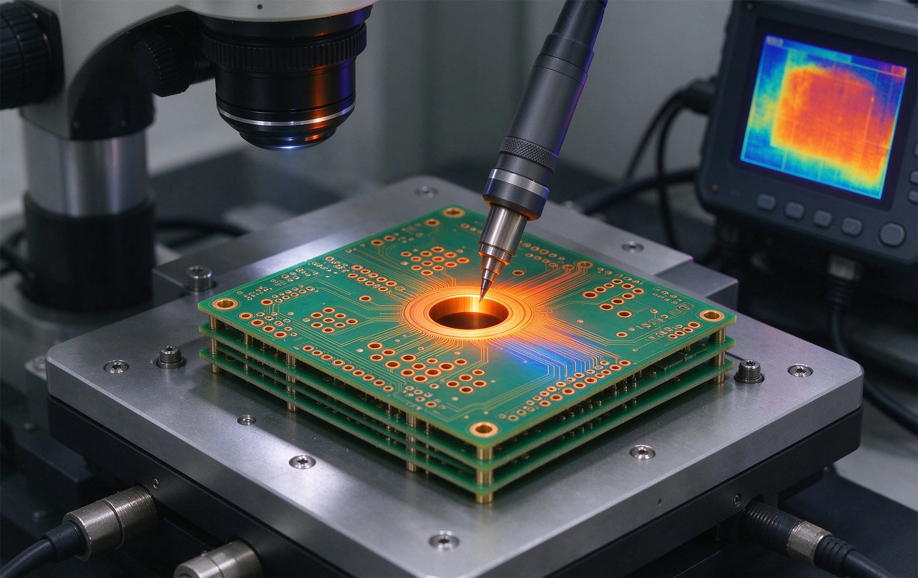
Backdrilling is a manufacturing process that removes the unused portion of a Plated Through-hole (PTH) via after initial board fabrication. A standard PCB via is drilled all the way through the board stack, with copper plating on the barrel walls connecting all layers. In many designs, you only need the via to connect the first few layers, not all of them. The remaining copper barrel—the stub—becomes a parasitic element that resonates at certain frequencies, degrades signal quality, and creates impedance mismatches.
In high-speed digital designs, backdrilling addresses these Signal Integrity problems by drilling out the stub from the blind side of the board, leaving only the portion of the via that actually carries the signal. Standard backdrilling typically removes stubs ranging from 0.2mm to 1.5mm beyond the deepest required layer.
For High Current applications, the motivation is different but the geometry is the same. In Power Electronics, you might have a 12-layer board where your main current path runs from layer 1 to layer 5, with layers 6 through 12 reserved for signal routing or ground planes. The portion of the via barrel extending from layer 5 to layer 12 is dead weight—and more than that, it's a potential problem spot.
High Current vias face a different set of challenges than their signal counterparts. Current Density, Thermal Management, and electromigration all interact in ways that can compromise via reliability over time. When you add a stub to this equation, you're introducing several potential failure modes:
Current flowing through a via generates heat. The resistance of the copper barrel, while low, isn't zero—and at high currents, even small resistances compound. A stub that extends beyond the current-carrying portion of the via creates a thermal discontinuity. Heat concentrates at the junction where current transitions from the barrel to the pad, and the stub itself may have hotspots where eddy currents or uneven Current Distribution create localized heating.
In boards operating near their thermal limits, these localized hotspots can push temperatures above the glass transition temperature (Tg) of the laminate, leading to pad lift, barrel cracking, or delamination over time. The effect is subtle initially—you might see it as intermittent failures in accelerated life testing—but it becomes a Field Reliability issue.
Current doesn't distribute evenly across a via barrel. It tends to crowd around the periphery, particularly at the entry and exit points where the via meets the pad. This phenomenon, known as Current Crowding, becomes more pronounced in stubs because the discontinuous geometry forces current to transition abruptly. The resulting hotspots accelerate copper migration and can lead to void formation within the barrel— voids that grow over thermal cycles until the via fails open.
High current PCBs often use vias as part of a Power Distribution network (Pdn). Whether you're distributing 12V from a regulator to processors or carrying 48V from a connector to a motor driver, the Pdn's impedance profile matters. Stubs act as resonant stubs in the transmission line sense—they reflect signals at specific frequencies determined by their length and dielectric properties.
In Power Distribution, these reflections don't manifest as bit errors the way they do in digital signals. Instead, they appear as voltage ripple, switching noise, and reduced decoupling effectiveness. If your high current path shares the board with sensitive analog or RF circuits, stub resonances can couple into those circuits through shared reference planes, creating noise issues that are difficult to debug.
Electromigration—the movement of copper atoms under the influence of current flow—is a known failure mechanism in semiconductor interconnects, but it affects PCB vias too, particularly at high current densities. The threshold for electromigration in PCB copper is higher than in semiconductor metallurgies, but it's not infinite. A via operating at current densities above approximately 25,000 A/cm² over extended periods is at risk.
Stubs complicate this picture by creating non-uniform Current Density distributions. The Current Crowding effect at via transitions concentrates electromigration-driving current at the worst possible locations—near the pad/barrel junction where failures are hardest to detect and most catastrophic when they occur.
Backdrilling eliminates the stub, which removes the geometry that causes thermal concentration, current crowding discontinuities, and resonant behavior. For high current applications, the benefits are practical:
These benefits are most pronounced in high current designs where the board operates continuously at elevated temperatures, or where the PDN shares real estate with noise-sensitive circuits.
Not all backdrilling is equal, and for high current vias, manufacturing tolerances matter more than they might for pure signal applications. Here's what you need to specify clearly with your manufacturer:
Backdrilling removes copper from the barrel using a larger drill bit than the original via drill. The over-travel beyond the target layer is typically 0.15mm to 0.25mm, but this varies by manufacturer and must be specified. For high current vias where every micron of barrel copper counts, confirm that the backdrill depth tolerance is acceptable—some manufacturers quote ±0.1mm, others ±0.2mm or looser.
You also need to specify the backdrill size relative to the original via. A common rule is to use a backdrill bit 0.15mm to 0.25mm larger than the original via drill. Going larger reduces the risk of leaving copper islands, but it also removes more barrel copper at the target layer, which matters if you're tight on Annular Ring dimensions.
Define maximum acceptable stub length based on your frequency content and current level. For very high current designs, even a 0.3mm stub can create measurable issues. Work with your manufacturer to determine the minimum over-travel they can reliably achieve, and verify that the resulting stub length meets your requirements.
When you backdrill a via, you create a stepped barrel profile. The remaining barrel copper (the current-carrying portion) must be properly supported by the capture pad on the target layer and constrained by the anti-pad in non-target layers. If the anti-pad clearance is too small, the backdrill may damage adjacent plane layers. If the capture pad is too small, you lose current-carrying capability at the critical termination point.
High current vias typically require heavier copper plating than standard impedance-controlled vias. A typical high-current via might use 1oz to 2oz copper plating (35µm to 70µm), compared to the 0.5oz to 1oz common in standard boards. Backdrilling removes some of this plating during the drilling process, which can reduce the effective barrel thickness in the backdrilled zone. Confirm with your manufacturer that the post-backdrill plating integrity meets your current-carrying requirements.
Backdrilling solves real problems, but it introduces complexity and cost. Before defaulting to backdrilling for all high current vias, consider these limitations:
Backdrilling is performed from one side of the board only—the side opposite the original drilling. This means you can only backdrill to a target layer that's not the bottom layer (for standard processing). If your current path requires connections to multiple internal layers from both sides of the board, backdrilling options become constrained.
Backdrilling adds a manufacturing step, which means additional cost and typically longer lead times. For high current boards where you might have dozens or hundreds of vias requiring backdrilling, the cost adder can be significant. Get a clear quote from your manufacturer before committing to a backdrilled design—sometimes a design revision to reduce via count or optimize layer assignment costs less than blanket backdrilling.
Depending on your application, alternatives to backdrilling may be more appropriate:
For boards where high current vias operate near thermal limits, simulation is worth the investment. Finite element analysis (FEA) tools can model current density distribution in vias, predict hotspot locations, and evaluate the effectiveness of backdrilling. Some PCB analysis tools now include integrated thermal-electrical simulation that can help you identify which vias need backdrilling and which don't.
Physical verification is equally important. Resistance measurements on fabricated boards—comparing the resistance of backdrilled vias to theoretical values based on barrel dimensions—can catch manufacturing issues before boards go into testing. A via that measures 20% higher resistance than expected suggests plating issues, barrel voids, or incorrect backdrill depth.
If you decide backdrilling is the right approach for your High Current Design, keep manufacturability in mind from the start:
High Current PCB backdrilling is not a universal solution, but it addresses real problems in Power Electronics where via stubs create thermal discontinuities, current crowding, and PDN noise. The technique is mature and widely available from capable manufacturers, but it requires careful specification and verification to deliver reliable results.
The decision framework is straightforward: if your board carries sustained high currents (10A or more per via), operates near thermal limits, or shares the board with noise-sensitive circuits, backdrilling is worth evaluating seriously. If your current requirements are moderate and thermal margins are comfortable, the added cost and complexity may not be justified.
As power electronics continue to push toward higher current densities in smaller packages—driven by electric vehicles, renewable energy systems, and dense power conversion—the role of backdrilling in reliable Pcb Design will only grow. Getting the fundamentals right today prepares you for the denser, more demanding designs coming tomorrow.
Backdrilling is a controlled drilling process that removes the unused portion of a plated through-hole via beyond the deepest required layer. It eliminates the via stub, reducing signal distortion in high-speed designs and improving thermal/current distribution in high-power applications.
Backdrilling itself doesn't reduce the current-carrying capacity of the via on the layers where it's needed. The portion of the barrel that carries current remains intact. However, the process removes plating in the stub area, which is not part of the current path anyway. Some reduction in Annular Ring may occur at the target layer if backdrill clearance is tight, which should be considered in pad design.
Current-carrying capacity depends on via size, copper plating thickness, temperature rise tolerance, and acceptable current density. As a rough guideline, a 0.6mm diameter via with 1oz copper plating can typically carry 2A to 3A safely. Larger vias with heavier plating can carry proportionally more. Always run a thermal simulation for your specific design conditions rather than relying on general rules.
Backdrilling typically adds 10% to 30% to PCB Fabrication cost, depending on the number of backdrilled vias, the complexity of the board, and the manufacturer's capability. The largest cost drivers are setup time for backdrill operations and the additional drill bits required. Grouping similar backdrill operations helps reduce cost.
No. Backdrilling requires specific equipment capabilities and process control that not all manufacturers have. Standard PCB fab houses focused on consumer electronics may not offer backdrilling. Look for manufacturers with experience in high-speed digital boards, RF boards, or aerospace/defense electronics—these shops typically have the equipment and process knowledge needed for reliable backdrilling.
Contact us to discuss your requirements.
High Current PCB Current Crowding: Sharp Corners vs. Teardrop TransitionsSeptember/03/2026
Overcoming Voltage Drop in High Current PCB Power Planes: A Case StudyJuly/13/2026
High Current PCB Grounding: Star Ground vs. Ground Plane in High Current PathsJuly/31/2026
High Current PCB Surface Finish: ENIG vs. HASL for High Current PadsSeptember/23/2026
High Current PCB Solder Wicking: Tented Vias vs. Untented ViasSeptember/01/2026
High Current PCB Ceramic Substrates: DBC vs. AMB Performance ComparisonOctober/14/2026
High Current PCB Routing: 45-Degree Angles vs. Curved Traces in PracticeJuly/12/2026
High Current PCB Edge Connectors: Current Rating and Thermal LimitsSeptember/20/2026