

Data centers consume enormous quantities of electrical power, and the infrastructure that distributes that power throughout the facility depends on components that must operate reliably under sustained High Current loads. The power shelf—the rack-mounted unit that houses power conversion and distribution circuitry—sits at the heart of this infrastructure, and the PCBs within it face design challenges that differ substantially from those of conventional circuit boards. Designing these boards demands a thorough understanding of thermal behavior, Current Carrying Capacity, voltage regulation under dynamic load, and the mechanical stresses that arise from both Thermal Cycling and physical mounting. Engineers who approach High Current PCB design for power shelves with the same techniques used for signal boards will encounter failures that range from subtle performance degradation to catastrophic overheating.
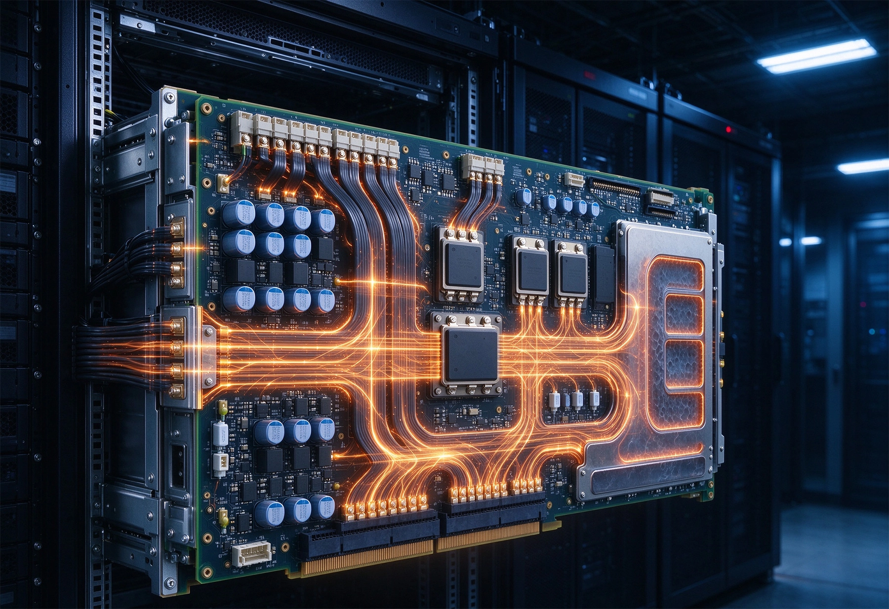
A modern data center power shelf typically operates at 48 volts nominal, distributing power to downstream DC-DC converters that serve individual server nodes. This 48V intermediate bus architecture has become the standard for high-density deployments because it allows current levels to be managed at the distribution level while keeping conductor sizes practical. The PCB within the power shelf must carry currents that can exceed several hundred amperes in larger systems, routing power from input connectors through rectification and power factor correction stages to the output bus that feeds server racks.
The current demands on these boards are not static. Modern data centers operate under highly dynamic load conditions as server utilization fluctuates throughout the day and across workloads. A power shelf PCB must maintain stable voltage regulation even as current draw transitions rapidly between light load and full load conditions. This dynamic behavior places additional demands on the board's Thermal Management infrastructure because peak currents during load transients can generate brief but intense heating that stresses both the PCB substrate and the components mounted on it.
The board must also accommodate the physical presence of large magnetic components—inductors and transformers—that are integral to the power conversion process. These components are heavy, generate their own heat, and create mechanical stress on the board during Thermal Cycling. The Pcb Design must provide adequate mechanical support, appropriate thermal paths away from heat-sensitive circuitry, and sufficient clearance to prevent corona discharge at high altitudes or in high-humidity environments.
Heat is the governing constraint in High Current PCB design. Every conductor carrying current generates heat according to the power dissipation equation, and at the current levels found in power shelves, this heat generation is substantial. The PCB itself becomes part of the Thermal Management system, and the design choices made during board layout have a direct and measurable impact on operating temperatures throughout the assembly.
Thermal Relief Patterns around component pads serve a critical function in High Current designs. While thermal reliefs—small spokes connecting a pad to the surrounding plane—are commonly used to facilitate soldering, they also influence how heat flows from hot spots to cooler regions of the board. In high current designs, oversized thermal reliefs can become significant sources of localized heating, and the designer must balance manufacturing solderability requirements against thermal performance. In many cases, Heavy Copper plating of the affected layers provides a better solution than relying on large thermal relief spokes.
Thermal Vias play an essential role in transferring heat from the surface layers of the PCB to internal planes or to mounting hardware that provides a thermal path to a heatsink or chassis. For high current power stages, thermal via arrays beneath MOSFETs, controllers, and inductors must be designed with adequate density and plating thickness to provide meaningful thermal conductance. The Thermal Resistance of the via array should be calculated as part of the overall thermal budget for the design, not treated as an afterthought.
The Layer Stackup in a power shelf PCB must be designed to accommodate high current carrying requirements alongside the signal routing needs of control circuitry. Standard PCB substrates such as FR-4 are acceptable for lower current sections, but the high current paths demand specialized approaches. Heavy Copper construction—typically 2 oz to 4 oz per square foot, and in some cases even heavier—is standard for the Power Planes that carry the bulk of the current. Some designs use copper weights up to 10 oz for the heaviest current paths, though this creates manufacturing challenges related to plating uniformity and drilling.
A typical high current power shelf PCB might employ four to eight layers, with dedicated Power Planes sized to carry the full load current and distribute it to component footprints. The power planes should be continuous where possible, with routing channels cut only where necessary and compensated by adding copper in adjacent areas to maintain consistent cross-sectional area. Any narrowing of the current path creates a localized hot spot that accelerates both conductor degradation and nearby component failure.
The dielectric thickness between power planes and ground planes affects both electrical performance and thermal spreading. Thinner dielectrics increase capacitance between planes, which helps suppress switching noise in power conversion circuitry, but they also reduce the Thermal Resistance between heat-generating components and any heatsinking structure mounted on the board. Designers must optimize this tradeoff based on the specific switching frequencies and thermal environment of the target application.
In many power shelf designs, the PCB alone cannot provide sufficient Current Carrying Capacity for the main power paths without unacceptable temperature rises. The solution is to integrate busbars—solid copper bars that bolt or weld directly to the PCB at termination points—into the overall current path. Busbars provide a low-resistance, high-current pathway that keeps operating temperatures within acceptable limits while allowing the PCB to handle the lower-current signal and control functions.
The interface between the busbar and the PCB is a critical design junction. The mechanical connection must maintain low contact resistance over the operational lifetime of the equipment, which may span many years of continuous service. Vibration, thermal cycling, and oxidation all threaten the reliability of this connection. Press-fit terminals, soldered busbar attachments, and bolted connections each offer different tradeoffs in cost, manufacturability, and long-term reliability, and the choice depends on the current levels involved, the expected thermal environment, and the mechanical robustness requirements of the application.
Some power shelf designs employ a hybrid approach where the PCB carries lower-Current Distribution and control signals while busbars handle main current paths. Others integrate busbars directly into the PCB construction using a process sometimes called embedded bus technology, where solid copper bars are laminated into the board structure and connected to internal planes through plated through-holes. This approach simplifies mechanical assembly and improves Current Distribution but adds complexity to the PCB Fabrication process.
Power shelves must maintain output voltage within tight tolerances despite significant load variations. The voltage regulation challenge is particularly acute at the high current levels found in data center applications, where load steps can occur rapidly and demand immediate response from the power conversion circuitry. The Pcb Design influences voltage regulation performance through several mechanisms, including the impedance of the current carrying planes and the placement and sizing of decoupling capacitors.
The impedance of the Power Distribution network on the PCB should be modeled and minimized as much as practical. At high current levels, even small resistances in the power path translate to meaningful voltage drops that degrade regulation performance. Wide, short traces for high current paths are preferable to narrow, longer routes, and the use of dedicated power planes rather than routed traces provides the lowest impedance path for current distribution. Parallel planes on multiple layers further reduce effective resistance and improve current sharing across the board.
Decoupling capacitors must be placed close to the loads they serve, with short, wide connections to the power and ground planes. In high current designs, the inductance of the capacitor connections is as important as the capacitance value itself, because inductive parasitics limit the effectiveness of the decoupling network during rapid current transients. Via-in-pad construction, where the Decoupling Capacitor mounts directly over a Plated Through-hole that connects to the internal plane, minimizes Loop Inductance and maximizes high-frequency decoupling performance.
Data center power shelves are expected to operate continuously for years without intervention, and the PCB must be designed to survive this extended service life without degradation. Thermal cycling is one of the primary wear mechanisms for power shelf PCBs, causing fatigue in solder joints, vias, and any dissimilar material interfaces within the board. The coefficient of thermal expansion mismatch between copper, substrate, and components creates stress during temperature changes, and designs that minimize the number of thermal cycles and the magnitude of temperature excursions will generally exhibit longer field life.
Via fatigue is a common failure mode in high current PCBs, particularly in Thermal Vias that carry significant current. Current Crowding at the barrel of the via creates localized heating that accelerates electrochemical migration and eventually causes the via to open. Designs that distribute current across multiple vias rather than concentrating it in a single large via reduce the Current Density in any one hole and extend via lifetime. Filled and capped vias provide better current handling and reduce the risk of void formation that can lead to premature failure.
Conformal coating can extend the life of power shelf PCBs by protecting the board surface from moisture, dust, and contamination that can lead to leakage currents and surface corrosion. In data center environments where air quality may vary depending on filtration effectiveness, conformal coating provides an additional margin of protection that is particularly valuable for boards operating at high voltage potentials.
What Copper Weight is typically required for high current power shelf PCBs?
Power planes typically use 2 oz to 4 oz copper as a baseline, with the heaviest current paths often requiring 6 oz to 10 oz. The specific requirement depends on the current level, acceptable temperature rise, and the thermal environment of the final installation.
How do you manage thermal expansion stress in High Current Pcb designs?
We use materials with compatible coefficients of thermal expansion, incorporate stress-relieving features such as routed slots around large component footprints, and apply conformal coating to protect the board surface from moisture-induced corrosion that can accelerate fatigue failures.
Can thermal simulation tools help optimize High Current Pcb designs before fabrication?
Absolutely. Thermal simulation of the complete power shelf assembly—including the PCB, busbars, Heat Sinks, and airflow—provides valuable insight into operating temperatures and allows design adjustments that would be impractical to make after prototypes are built.
What reliability testing do you perform on high current power shelf PCBs?
Our qualification process includes thermal cycling, power cycling, high-current stress testing, and extended burn-in at elevated load to verify that the design meets its expected service life targets before entering volume production.
How do you handle the mechanical integration of busbars with PCB assemblies?
We specify bolted or press-fit connections designed for the specific current levels and mechanical requirements, using materials and torque specifications that maintain low contact resistance throughout the product's operational life under data center environmental conditions.
Contact us to discuss your requirements and learn how our expertise in High Current Pcb Design supports reliable power shelf development for data center applications.
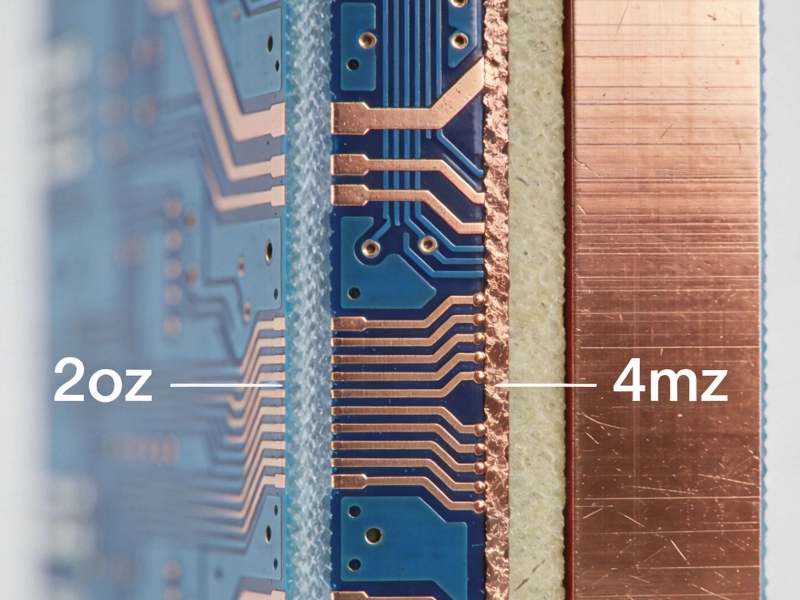
2oz vs. 4oz Copper: Which is Best for Your High Current PCB?July/10/2026
High Current PCB Design for Industrial Motor DrivesSeptember/28/2026
High Current PCB Thermal Vias: Array Spacing and Heat Transfer EfficiencySeptember/15/2026
High Current PCB Design for Telecommunications Base StationsSeptember/18/2026
High Current PCB Design for Electric Forklifts: A Practical Engineering GuideOctober/13/2026
High Current PCB Thermal Relief: Full Connect vs. Modified SpokesJuly/16/2026

High Current PCB Design for Railway Traction SystemsAugust/07/2026
Designing a High Current PCB Motor Driver: Avoiding EMI PitfallsJuly/14/2026