

Designing Power Electronics for high-speed trains is a discipline where failure is not an option. Unlike consumer electronics, where a reboot might fix a glitch, a failure in a train's auxiliary power system can lead to significant operational delays, safety hazards, and massive financial losses. At the heart of these systems lies the Printed Circuit Board (PCB), which must manage substantial electrical loads while withstanding extreme environmental stress. Therefore, mastering High Current PCB Design for High-Speed Train Auxiliary Power is essential for engineers working in the rail transit sector.
The auxiliary power unit (APU) is responsible for converting the high voltage from the catenary or third rail into stable, lower voltages required for lighting, air conditioning, door control systems, and battery charging. These circuits often handle currents ranging from 50A to over 200A. In this article, I will share my practical experience and technical insights on how to design robust PCBs for these demanding applications, ensuring compliance with stringent industry standards like En 50155.
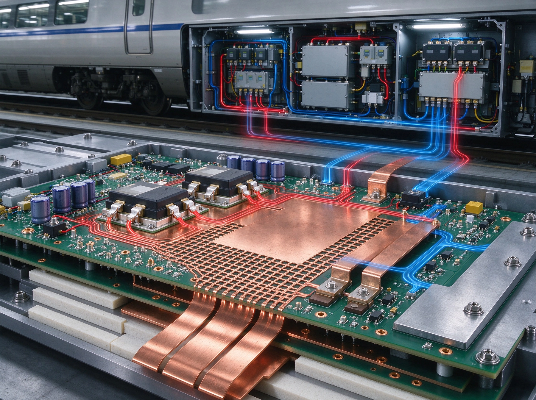
Before we dive into the layout techniques, it is crucial to understand the environment in which these boards operate. High-speed trains are subject to violent vibrations, wide temperature fluctuations (from -40°C to +70°C or higher), and significant electromagnetic interference (Emi). A standard commercial Pcb Design will fail quickly under these conditions.
The auxiliary power system acts as the lifeblood of the train's non-traction loads. It typically involves DC-DC converters or inverters that step down the 1500V or 25kV input to usable levels like 110V DC or 380V AC. Because these conversion processes involve high switching frequencies and high currents, the PCB must handle significant thermal loads. If the High Current PCB Design for High-Speed Train Auxiliary Power is not optimized for Thermal Management, the board will suffer from delamination or trace burnout.
Handling High Current on a PCB is not just about making traces wider. It requires a holistic approach involving Copper Weight selection, thermal relief, and advanced interconnect technologies.
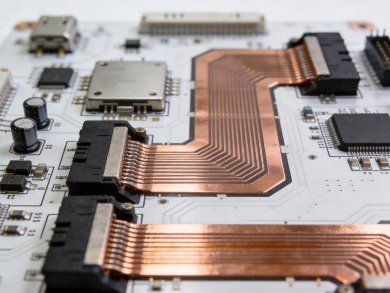
The most fundamental rule in High Current Design is ensuring the copper cross-section is sufficient to carry the load without excessive temperature rise. While standard PCBs use 1oz (35µm) copper, High Current designs for trains often require 4oz, 6oz, or even 10oz copper weights.
Sometimes, increasing Copper Weight is not enough, or it makes the manufacturing process too difficult (e.g., etching thick copper leads to undercutting issues). In such cases, we employ Embedded Copper coins or press-fit busbars.
Embedded Copper coins are blocks of solid copper inserted into the PCB cavity. They provide a low Thermal Resistance path and can carry massive currents directly. For the auxiliary power modules I have designed, using busbars for the main DC link connections reduced the Pcb Trace current load by 60%, significantly improving reliability. This is a critical technique in High Current Pcb Design for High-Speed Train Auxiliary Power.
For components like MOSFETs and IGBTs that generate significant heat, Thermal Vias are essential. These vias connect the component's Thermal Pad to internal ground planes or bottom-layer copper pours. However, one must be careful with via tenting. In high-current applications, vias carrying current should be plugged and plated over to prevent Solder Wicking during assembly, which could weaken the joint.
Designing for current is one thing; ensuring the board survives the train's lifecycle is another. The En 50155 standard specifies the electronic equipment used on rolling stock. Compliance is mandatory.
Standard FR-4 material is often insufficient for the high temperatures encountered in train underfloor compartments. We specify High Tg (Glass Transition Temperature) materials, typically Tg > 170°C. Furthermore, Conductive Anodic Filament (CAF) resistance is vital. CAF is a failure mode where copper salts grow along the glass fiber bundles inside the PCB, causing shorts. Using CAF-resistant resin systems and ensuring adequate spacing between high-voltage nets is a non-negotiable part of the design process.
High-speed trains vibrate intensely. Large components, such as capacitors and heavy inductors used in the auxiliary power supply, exert significant mechanical stress on solder joints. To mitigate this:
Modern design workflows rely heavily on simulation. Before fabricating a prototype, we run Thermal and Ir Drop simulations.
Ir Drop simulation helps us identify areas where the voltage drop is too high, which indicates potential hotspots. If the simulation shows a voltage drop of more than 2% on the main power rail, we iterate the design, perhaps adding more vias or widening traces. It is common that junior engineer might ignore the Via Current Capacity, but actually a single via can usually only carry about 1A safely. We need many vias in parallel for high current paths. This simulation step is indispensable for successful High Current Pcb Design for High-Speed Train Auxiliary Power.
Designing PCBs for high-speed train auxiliary power systems is a complex interplay of Electrical Engineering, Thermal Management, and mechanical robustness. By adhering to standards like EN 50155, utilizing advanced manufacturing techniques like embedded copper, and rigorously simulating thermal performance, we can create systems that are safe and reliable. As trains become faster and more electrified, the demand for superior High Current Pcb Design for High-Speed Train Auxiliary Power will only continue to grow.
The creepage distance depends on the operating voltage and the pollution degree defined in EN 50124-1. For high-voltage auxiliary systems, designers often need to account for creepage distances of several millimeters to prevent arcing, sometimes requiring slots or cutouts in the PCB.
IPC-2152 is a newer standard that provides more accurate current-carrying capacity calculations by considering the board's thermal conductivity, thickness, and the presence of internal planes. Ipc-2221 is based on older data and often leads to over-designed or under-designed traces.
Emi is managed by minimizing loop areas for high di/dt paths, using ground planes effectively, and placing filtering capacitors close to switching nodes. Shielding Cans may also be used over sensitive control circuitry.
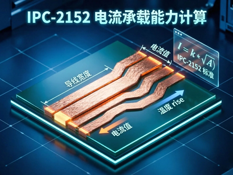
Mastering IPC-2152 Current Carrying Capacity Calculation for Reliable PCB DesignJune/04/2026
High Current PCB Design for High-Frequency Switching RegulatorsSeptember/04/2026
High Current PCB Current Sensing: Shunt Resistor vs. Hall Effect LayoutJuly/29/2026
Designing a High Current PCB Motor Driver: Avoiding EMI PitfallsJuly/14/2026
A Deep Dive into High Current PCB Design for Solar InvertersJuly/17/2026
High Current PCB Design for Renewable Energy MicrogridsSeptember/30/2026
High Current PCB Design for Robotics Motor ControllersSeptember/16/2026
High Current PCB Design for Aerospace Power DistributionSeptember/08/2026