

Induction heating is one of those applications where the electrical demands push PCB technology to its practical limits. A high-power induction heater operating at tens or hundreds of kilohertz must deliver substantial current through the PCB while managing heat that can destroy the board if not handled properly. The design challenges include not just the obvious issues of trace width and Copper Weight, but subtler problems like skin effect at high frequencies, proximity effect in parallel conductors, and the interaction between the resonant tank circuit and the Pcb Layout that determines efficiency and reliability. Engineers who successfully design PCBs for induction heating applications develop an intuition for these challenges that comes only from understanding the underlying physics and from debugging the failures that occur when the physics are ignored.
This article provides a comprehensive guide to High Current PCB design for induction heater applications, covering the electrical requirements, the Thermal Management challenges, the layout strategies that determine performance, and the practical design decisions that separate working designs from smoke-filled disappointments. Whether you are designing your first induction heater PCB or looking to improve an existing design, the principles and practices described here provide a foundation for reliable high-power performance.

Induction heaters work by inducing eddy currents in a conductive workpiece through an alternating magnetic field. The power delivered to the workpiece depends on the current flowing through the induction coil, and more specifically on the Current Density in the coil conductors. Higher current means stronger magnetic fields and more power transfer to the workpiece. The relationship is roughly quadratic: doubling the current quadruples the power transfer, which is why induction heaters push for the highest practical current levels in their coil designs.
A typical desktop induction heater might operate at 15 to 30 amps through the coil. Larger industrial units push to 100 amps or more. At these current levels, the PCB must carry substantial current from the Power Electronics to the coil terminals, and any resistance in the current path converts electrical energy directly to heat. The heating effect follows Ohm's law: power dissipated in a conductor equals current squared times resistance. At 30 amps, a mere 10 milliohms of resistance dissipates 9 watts of heat. At 100 amps, that same 10 milliohms dissipates 100 watts. These are not trivial heat loads for a PCB to manage.
The frequency of operation adds another dimension to the current challenge. Induction heaters typically operate in the 100 kHz to 500 kHz range, and some designs push toward 1 MHz or higher. At these frequencies, skin effect becomes significant. Skin effect forces alternating current to flow near the surface of the conductor rather than uniformly across the cross-section, effectively reducing the current-carrying area and increasing the effective resistance. A 4-ounce Copper Trace that would comfortably carry 30 amps of DC current may overheat at 30 amps of 300 kHz AC because the skin depth at that frequency reduces the effective cross-section dramatically.
The starting point for High Current PCB design is selecting the appropriate Copper Weight and designing Trace Geometry that can carry the required current without excessive temperature rise. The relationship between current, Trace Geometry, and temperature rise is well-understood empirically, and several design guidelines provide starting points for the design process.
Copper weight, expressed in ounces per square foot, determines the thickness of the copper conductor. Standard PCB copper is 1 ounce per square foot, which corresponds to approximately 35 microns or 1.4 mils. For High Current applications, heavier copper weights like 2 ounce, 3 ounce, or even 6 ounce are commonly used. Each doubling of copper weight approximately doubles the current-carrying capacity for a given trace width and temperature rise allowance, though the relationship is not perfectly linear due to thermal factors.
Trace width must be sized based on the current, the copper weight, the acceptable temperature rise, and the available board area. Ipc-2221, the generic standard for Pcb Design, provides current-carrying capacity charts that relate current to trace width for different copper weights and temperature rises. These charts are useful starting points, but they are based on DC current and room temperature conditions. For induction heating applications with AC current and elevated operating temperatures, more conservative design margins are appropriate.
For High Current traces, wider traces are generally better than thicker copper alone. A trace that is 100 mils wide with 2-ounce copper has more surface area for Heat Dissipation than a trace that is 50 mils wide with 4-ounce copper, even though both have approximately the same cross-sectional area. The wider trace can dissipate more heat to the surrounding air and substrate, making it more effective at managing the temperature rise. Designing with wider traces rather than relying solely on copper weight is often the better strategy for Thermal Management.
At the frequencies used in induction heating, skin effect fundamentally changes how current flows in a conductor and how the PCB must be designed to handle the resulting losses. Ignoring skin effect leads to designs that appear adequate by DC current calculations but overheat in actual operation.
Skin depth describes how deeply current penetrates into a conductor at a given frequency. At DC, current flows uniformly across the entire cross-section. At high frequency, the Current Density is highest at the surface and decreases exponentially toward the interior. The skin depth is defined as the depth at which the current density has fallen to approximately 37% of its surface value. Below this depth, the contribution to current flow is minimal.
For copper at room temperature, the skin depth at 100 kHz is approximately 0.2 mm or about 8 mils. At 300 kHz, the skin depth drops to about 0.12 mm or 4.7 mils. At 500 kHz, it is approximately 0.09 mm or 3.6 mils. These skin depths are smaller than the thickness of even standard 1-ounce copper, which means that at typical induction heating frequencies, the current flows only in the outer portion of the copper and the inner portion of the trace contributes little to current conduction.
The practical implication for Pcb Design is that increasing Copper Thickness beyond about twice the skin depth provides diminishing returns for current capacity. A 6-ounce Copper Trace at 300 kHz has most of its current flowing in the outer 2 to 3 mils, and the additional Copper Thickness beyond the skin depth primarily serves as a thermal mass rather than additional current-carrying capacity. For the highest frequency designs, using very wide traces with moderate copper weight may be more effective than using thick copper with narrow traces.
Managing heat in High Current Pcb designs is not optional. The PCB substrate, typically FR4 or a similar composite, degrades rapidly above its glass transition temperature, and the solder joints connecting components lose mechanical integrity as they approach their melting points. Effective thermal management keeps the board within safe operating temperatures throughout the operating range.
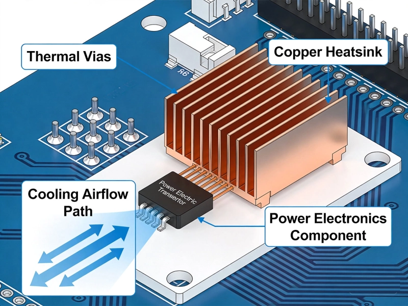
Thermal Vias provide a path for heat to flow from the high-current traces to an internal ground plane or to a heatsink attached to the board surface. When high-current traces are routed over ground planes, adding Thermal Vias near the trace reduces the Thermal Resistance between the trace and the plane, spreading the heat across a larger area. The thermal vias act as small heat pipes, conducting heat away from the hot trace to wherever the plane is connected to a heatsink or to ambient air through the board edge.
Heatsinking the PCB itself is often necessary for induction heater designs. Aluminum-backed PCBs, sometimes called metal core PCBs or IMS substrates, provide a thermal path directly to an aluminum backing plate that can be connected to an external heatsink or forced-air cooling system. The thermal conductivity of aluminum, approximately 200 W/mK, is orders of magnitude higher than FR4 at 0.3 W/mK, providing dramatic improvement in heat spreading and dissipation. Metal core boards cost more than standard FR4 boards but are essential for high-power designs where the heat load exceeds what FR4 can dissipate.
Component Placement affects thermal distribution across the board. Heat-generating components like MOSFETs, IGBTs, and the resonant capacitor bank should be positioned to facilitate heat spreading rather than creating localized hot spots. Placing high-heat components near the board edge, where air circulation is better, reduces the Thermal Resistance to ambient. Distributing multiple heat sources across the board rather than clustering them in one area allows each to have better access to cooler regions of the board.
The resonant tank in an induction heater consists of the induction coil and the resonant capacitor bank, connected in a series or parallel configuration that creates resonance at the operating frequency. The layout of these components on the PCB is critical for efficiency and for minimizing unwanted parasitic effects that reduce performance.
Parasitic Inductance in the connections between the resonant capacitor and the induction coil directly subtracts from the effective inductance of the resonant circuit. Any Loop Area in the high-current tank circuit creates Parasitic Inductance that must be overcome by the Power Electronics, reducing efficiency and potentially causing excessive voltage stress on the switching devices. Minimizing Loop Area in the tank circuit is one of the most important layout priorities for induction heater designs.
The geometry of the tank circuit connections should use wide, short conductors with minimal spacing between the positive and return paths. When the positive and return conductors are close together and parallel, their magnetic fields partially cancel, reducing the Loop Inductance. Using wide traces or bus bars for the tank connections, rather than narrow traces, reduces the series resistance and inductance of the connections. The goal is to make the tank circuit connections as direct and as low-impedance as possible.
Capacitor bank placement relative to the switching devices affects the current waveform and the switching losses. The resonant capacitors should be mounted as close as possible to the switching devices to minimize the parasitic inductance in the switching loop. Long leads or traces between the switches and the capacitors allow voltage overshoot and ringing that increases stress on the semiconductors and generates electromagnetic interference. A compact, low-inductance layout between the switches and the capacitors is essential for clean switching and high efficiency.
The switching devices, typically MOSFETs or IGBTs, and their gate driver circuits determine how efficiently power is transferred to the resonant tank. The layout of these components and their interconnections has a direct and measurable impact on switching performance, efficiency, and electromagnetic emissions.
Gate drive loops should be kept as short and direct as possible. The gate driver must supply current to charge and discharge the gate capacitance of the switching device during each switching transition. Any inductance in the gate loop slows the transition, increasing switching losses and allowing the device to spend more time in the high-dissipation transition region. For devices switching at hundreds of kilohertz, even small inductances have significant impact on switching speed and losses.
The gate source voltage should be clean and well-controlled. Noise or ringing on the gate drive signal can cause false triggering, where the device turns on unexpectedly and creates a short circuit through the power path. Separate gate driver power supplies, bypassed with appropriate capacitors close to the driver, help ensure clean gate drive signals. In some designs, using separate gate and source sense pins on the switching device, with Kelvin connections to the driver, further improves the quality of the gate drive signal.
Power loop layout for the switching devices determines the switching commutation behavior. The power loop consists of the switching device, the DC bus capacitors, and the resonant tank connection. Minimizing the area of this loop reduces parasitic inductance that causes voltage overshoot when the device turns off. Voltage overshoot beyond the device rating can destroy the switch instantly, so controlling the power Loop Inductance is critical for reliable operation. Wide, closely-spaced conductors for the power loop, with the bus capacitors mounted as close as possible to the switching devices, minimize loop inductance.
The DC bus distributes power from the input supply to the switching devices and must handle substantial current with minimal loss. The DC bus design affects both the efficiency and the thermal performance of the power conversion stage.
DC bus conductors should be sized for the current they carry with appropriate margin for the RMS current, which may be higher than the average DC current depending on the duty cycle and waveform shape. Using wide copper traces or dedicated bus bars for the DC distribution reduces the resistance and the associated I-squared-R losses. The DC bus impedance also affects the quality of the voltage supply to the switching devices; a high-impedance bus allows voltage sag during current transients that can affect switching performance.
Bulk bus capacitance is essential for smoothing the DC voltage and providing energy storage for the switching transients. The capacitor bank should be mounted close to the switching devices to minimize the inductance between the capacitors and the switches. Using multiple capacitors in parallel reduces the effective ESL and ESR of the capacitor bank and provides better high-frequency performance than a single large capacitor. Ceramic capacitors with low ESL are particularly valuable for the high-frequency current demands of the switching transients.
Grounding for the power stage should be designed to minimize ground loops and to provide a clean reference for the control circuitry. The high currents flowing in the power stage can create voltage differences across the ground plane that affect the low-level signals in the control and measurement circuits. A star ground configuration, where the control ground is connected to the power ground at a single point, reduces these interactions and prevents the control circuits from seeing noise that could affect their operation.
The PCB substrate material affects both the electrical and thermal performance of the assembly. For induction heater designs, the choice of material involves trade-offs between thermal conductivity, dielectric properties, mechanical strength, and cost.
Standard FR4 is adequate for low-power induction heater designs where the heat load is modest and the frequency is below a few hundred kilohertz. The dielectric properties of FR4 are acceptable at these frequencies, and the cost and availability advantages are significant. However, FR4 thermal conductivity is poor at approximately 0.3 W/mK, which limits the heat spreading capability and constrains how much power can be handled before thermal issues become problematic.
High-Tg FR4 variants offer better thermal performance and higher temperature ratings than standard FR4. With Tg values above 150 degrees Celsius, these materials provide more margin against thermal degradation in demanding applications. Some high-Tg materials also incorporate thermal enhancement features that improve thermal conductivity while maintaining good electrical properties. These materials represent a practical middle ground between standard FR4 and more exotic options.
Metal core substrates, with aluminum or copper backing, provide the best thermal performance for high-power induction heater designs. The metal core provides a direct thermal path to a heatsink or to forced-air cooling, dramatically reducing the thermal resistance from the active components to the ambient. IMS substrates with thermal conductivities of 1 to 3 W/mK or higher can handle power densities that would destroy standard FR4 boards. The trade-off is higher cost and more limited design flexibility compared to standard multi-layer boards.
Ceramic Substrates like alumina or aluminum nitride offer excellent thermal conductivity along with good dielectric properties at high frequency. These materials are used in the most demanding high-power applications where the thermal demands exceed what metal core boards can handle. The cost is substantially higher than conventional PCB materials, and the manufacturing process is more specialized, which limits their use to high-value applications where the performance requirement justifies the investment.
Designing a High Current Pcb for induction heating must account for manufacturing capabilities and assembly requirements. Even the best electrical and Thermal Design is worthless if the board cannot be manufactured reliably or assembled without damage.
Copper weight availability limits what can be ordered from PCB fabricators. Standard copper weights of 1, 2, and 3 ounces are commonly available. Heavier weights like 4, 6, or 10 ounces may require special ordering and may come with longer lead times and higher cost. Designing to standard copper weights where possible simplifies procurement and reduces the risk of fabricator limitations causing delays or quality issues.
Trace spacing requirements for high voltage must be balanced against the need for wide traces in high current paths. As the operating voltage increases, the spacing between traces must increase to prevent arcing or tracking along the surface. The Creepage And Clearance requirements depend on the voltage level, the pollution degree of the operating environment, and the applicable safety standards. Designing the layout to accommodate adequate spacing while still providing wide current-carrying traces requires careful planning of the board geometry.
Component mounting for heat-generating devices must account for thermal relief during soldering. Heavy Copper areas dissipate heat rapidly during hand or reflow soldering, making it difficult to achieve good solder joint formation. Using Thermal Relief Patterns that connect the component pad to the surrounding copper with thin spokes allows the pad to reach soldering temperature without cooling too rapidly. After assembly, the thermal relief spokes provide adequate thermal connection for heat spreading.
Verifying that a High Current Pcb Design meets its electrical and thermal performance requirements is essential before committing to production. The combination of high current, high frequency, and significant heat generation creates failure modes that are difficult to predict accurately from simulation alone.
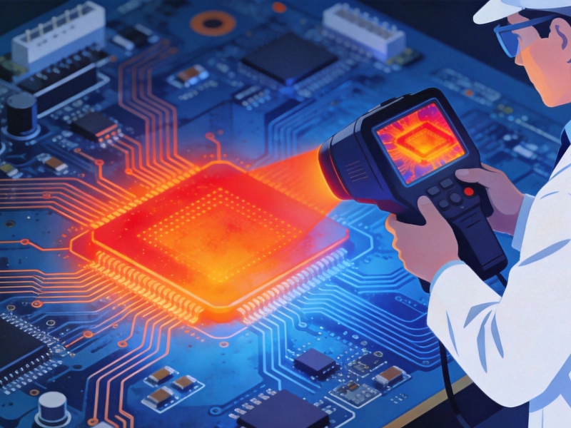
Thermal imaging with an infrared camera identifies hot spots on the board during operation, revealing areas where the Thermal Design is inadequate. Operating the board at rated current and observing the temperature distribution shows whether the thermal management strategy is working or whether certain areas are overheating. Thermal imaging should be performed at the maximum expected operating current and in the worst-case ambient temperature to verify that the design has adequate margin.
Electrical testing should verify the key parameters including the resonant frequency, the Q factor of the resonant tank, the switching waveforms at the gates and drains of the power devices, and the overall power efficiency. Any deviation from expected values indicates issues with component selection, layout, or parasitics that should be corrected before proceeding to full-power testing.
Long-term reliability testing under representative operating conditions reveals weaknesses that short-term testing might miss. Thermal Cycling, high-power operation over extended periods, and vibration testing if the application involves mechanical stress all contribute to understanding the design margins. The goal is to find and fix problems during development rather than discovering them in field failures.
Several predictable mistakes undermine high current PCB designs for induction heating applications. Understanding these common errors helps avoid them in your own work.
Underestimating the impact of skin effect is the most common mistake. Designers who calculate trace width based on DC current tables without accounting for high-frequency resistance often produce traces that are too narrow or too thin for the actual operating conditions. Always calculate the skin depth at the operating frequency and verify that the trace geometry provides adequate current-carrying capacity in the skin effect regime.
Neglecting thermal management until the layout is complete is another common error. Adding thermal features to a completed layout is difficult and may compromise the Electrical Design. Thinking about thermal management from the beginning, including Component Placement, Heatsink Mounting provisions, and thermal via placement, produces better integrated designs than treating thermal and electrical concerns as separate problems.
Failing to minimize loop areas in the resonant tank and switching circuits leads to poor efficiency and excessive voltage stress. Every inch of loop area in these high-frequency circuits translates to parasitic inductance that must be overcome or tolerated. Spending extra time on the layout to minimize these loop areas pays back in better performance and more reliable operation.
Using inadequate bus capacitance or placing the capacitors too far from the switching devices creates voltage transients that stress the semiconductors and reduce efficiency. The switching transients demand energy delivery at very high rates that only local capacitance can provide. The bulk capacitors can be relatively far from the switches, but the high-frequency bypass capacitors must be right at the device pins.
High Current Pcb Design for induction heating applications demands attention to electrical, thermal, and manufacturing considerations that are more demanding than most other PCB applications. The combination of high current, high frequency, and significant heat generation creates design challenges that cannot be solved by simply making traces wider or copper thicker. Understanding the underlying physics of skin effect, thermal conduction, and resonant circuit behavior provides the foundation for making informed design decisions.
The key principles for successful induction heater PCB design include sizing traces for high-frequency current rather than DC current, implementing effective thermal management from the beginning of the design process, minimizing loop areas in the resonant tank and switching circuits, and selecting materials appropriate for the power level and frequency of the specific design. Following these principles while iterating through thermal imaging and electrical testing produces designs that perform reliably at the power levels required for effective induction heating.
As induction heating continues to find new applications in industrial processes, consumer products, and Electric Vehicle systems, the demand for skilled designers who understand high current PCB design will continue to grow. Building expertise in this area provides valuable capabilities for addressing the power electronics challenges that are increasingly central to modern engineering.
Contact us to discuss your requirements and explore how our PCB design and manufacturing capabilities can support your high-power induction heating applications.
High Current PCB Design for High-Temperature Downhole ToolsOctober/28/2026
Designing a High Current PCB for Industrial Welding EquipmentJuly/23/2026
High Current PCB Design for Medical Imaging EquipmentSeptember/10/2026
Why Your High-Power PCBs Overheat (And the 5 Methods That Actually Fix It)May/20/2026
5 Critical Thermal Management Problems in High Power PCBsMay/21/2026
Designing a 100A High Current PCB for EV Battery Management SystemsJuly/09/2026
High Current PCB Design for Marine Battery SystemsSeptember/21/2026
Plated Through Hole Current Rating: Complete Guide for PCB DesignersMay/21/2026